S1F76640 Series
S1F70000 Series EPSON 2–45
Technical Manual
S1F76640
Series
POFF TC2 TC1 Temperature VREG CR Remarks
(Note 1) (Note 1) (Note 1)
Gradient CT(Note 2)
Output Oscillator —
1(VDD) Low(VSS) Low(VSS) –0.40%/ ˚C ON ON —
1(VDD) Low(VSS) High(VO) –0.25%/ ˚C ON ON —
1(VDD) High(VO) Low(VSS) –0.55%/ ˚C ON ON —
1(VDD) High(VO) High(VO) –0.55%/ ˚C ON OFF
Series connection (Note 4)
0(VSS) Low(VSS) Low(VSS) — OFF(Hi-Z)(Note 3) OFF —
0(VSS) Low(VSS) High(VO) — OFF(Hi-Z)(Note 3) OFF —
0(VSS) High(VO) Low(VSS) — OFF(Hi-Z)(Note 3) OFF —
0(VSS) High(VO) High(VO) — OFF(Hi-Z) ON
Boosting only (Note 5)
Note 1 : Please note that potentials on the High side are different between the POFF pin and TC2/TC1 pin.
Note 2 : The formula below is used to define temperature gradient C
T:
C
T =
V
REG (50˚C) – VREG (0˚C)
×
1
× 100 (%/˚C)
50˚C–0˚C V
REG (25˚C)
Example :When C
T=–0.6%/˚C is selected,
⋅ When Ta is 25˚C, the V
REG output becomes –8V at 25˚C.
∆V
REG/∆T=CT ⋅
VREG (25˚C)
=–0.6 × 10
–2
× 8=–48mV/˚C
When the temperature rises 1 ˚C, the
VREG value reduces by 48mV.
⋅ When V
REG is –10V at 25˚C, the formula below is formed:
∆
VREG ∆T=–60mV/˚C
Note 3 : At power off time (V
REG output : OFF, CR oscillator : OFF), the potential of the VO output is about
V
DD+0.5V.
Note 4 : When this mode is selected at a series connection, the first stage clock can drive the next stage IC and
this mode is effective for reducing the power consumption of the next stage IC. (See Figure 8.4)
Note 5 : Select this mode for boosting only. And the current consumption can be reduced.
Temperature Gradient Selection Circuit
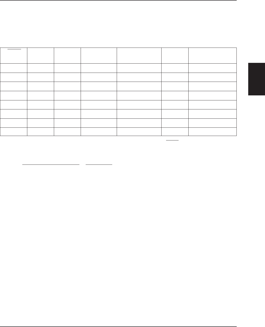
S1F76640 can provide three kinds of temperature gradients suitable for driving LCD to VREG output as shown
Table 5-1.
Table 5-1 Temperature Gradient Adaptation Table


