S1F70000 SeriesEPSON 6–1
Technical Manual
Appendix
Appendix
ABSOLUTE MAXIMUM RATINGS
Absolute maximum ratings are the maximum physical
and electrical ratings of a device beyond which perfor-
mance degradation or damage will occur. Always
check circuit conditions before using a device to avoid
exceeding these ratings. Typically, absolute maximum
ratings include the following parameters.
1. Power supply voltage
Steady state applied voltages, noise, reverse voltage
transients and power-on-transients can degrade or
damage the integrated circuit if they exceed the
maximum power supply voltage rating.
2. Input signal voltage
Input signals exceeding this rate can damage input
protection circuits
3. Output current
Generally, specifications are not set for CMOS
devices with small output currents. Devices that
provide large drive currents will have output cur-
rent specifications.
4. Power dissipation
The maximum power dissipation of a device is
limited by its construction and package type.
Maximum output current limits are set to prevent
thermal damage.
5. Operating temperature range
The temperature range for normal device operation
with no change in performance characteristics.
6. Storage temperature range
The temperature range for device storage with no
degradation or damage. This specification is par-
ticularly important when ICs are being transported
by air.
7. Soldering temperature and the duration
The maximum soldering temperature and the time
for which the leads can be at this temperature.
RECOMMENDED OPERATING
CONDITIONS
Recommended operating conditions are the conditions
under which a device functions correctly. These
include power supply voltage, input conditions and
output current. These conditions are sometimes listed
as part of the electrical characteristics.
ELECTRICAL CHARACTERISTICS
Electrical characteristics specify the DC and AC
characteristics of a device under the worst measure-
ment conditions.
POWER DISSIPATION CONDITIONS
To prevent damage always consider the following
points when designing with power regulation ICs.
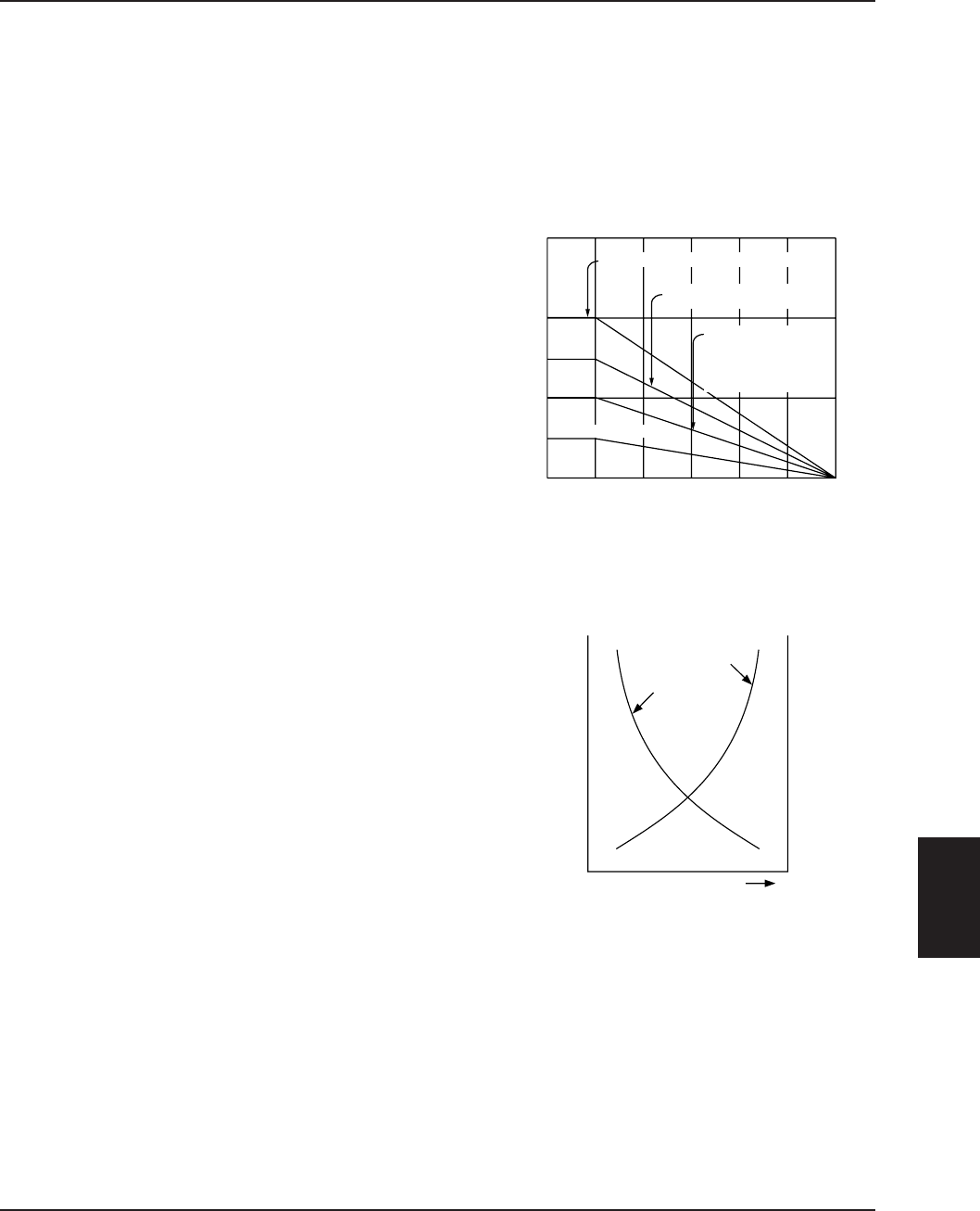
The following figure shows the cost and reliability
of a product and is significant when designing a
system.
50 100 150
Ambient temperature (˚C)
Power dissipation (W)
0
1
2
3
0.5 mm thick substrate
12.5 x 20 x 0.7 mm
3
ceramic substrate or
1.7 mm thick glass-epoxy
substrate with 1 cm
2
collector surface area
12.5 x 40 x 0.7 mm
3
ceramic substrate
25 x 80 x 0.7 mm
3
ceramic substrate
Junction temperature
Cost
Reliability
Reliability
Cost
1. A precise thermal design is necessary to ensure
adequate heat dissipation.
The following figure shows the power dissipation
capacity in relation to ambient temperature.


