S1F76610 Series
S1F70000 Series EPSON 2–11
Technical Manual
S1F76610
Series
FUNCTIONAL DESCRIPTIONS
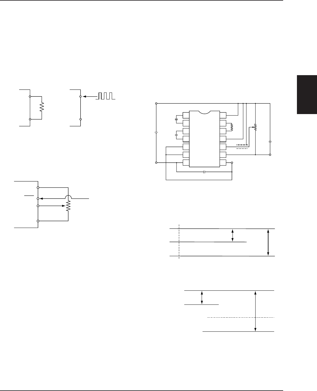
CR Oscillator
The on-chip CR oscillator network frequency is deter-
mined by the external resistor, R
OSC, connected be-
tween OSC1 and OSC2. This oscillator can be disabled
in favor of an external clock by leaving OSC2 open and
applying an external clock signal to OSC1.
OSC1
Oscillator External clock
External clock
signal
R
OSC
OSC2
OSC1
OSC2
Reference Volatge Generator and Voltage
Regulator
The reference voltage generator supplies a reference
voltage to the voltage regulator to control the output.
This voltage can be switched ON and OFF.
V
DD
V
REG
R
RV
= 100 kΩ to 1 MΩ
RV
P
OFF
Control signal
Voltage Multiplier
The voltage multiplier uses the clock signal from the
oscillator to double or triple the input voltage. This re-
quires three external capacitors–two charge-pump ca-
pacitors between CAP1+ and CAP1– and CAP2+ and
CAP2–, respectively, and a smoothing capacitor be-
tween V
I and VO.
C4
R1
R2
+
10 µF
V
REG
= –8 V
V
I
= –5 V
R
RV
100 kΩ
to
1 MΩ
R
OSC
1 MΩ
C1 +
10 µF
C2
5 V
+
10 µF
C3
+
10 µF
V
O
= –15 V
V
DD
= 0 V
14
13
12
11
10
9
8
1
2
3
4
5
6
7
Double voltage potential levels
V
CC
(+5V)
GND
(–5V)
V
DD
= 0 V
V
I
= –5 V
V
CAP2
– = 2V
I
= –10 V
Tripled voltage potential levels
VDD = 0 V
V
I = –5 V
V
O = 3VI = –15 V


