


S1F76640 Series
S1F70000 Series EPSON 2–43
Technical Manual
S1F76640
Series
FUNCTIONAL DESCRIPTIONS
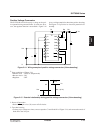
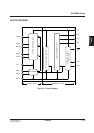
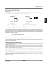
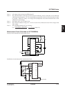
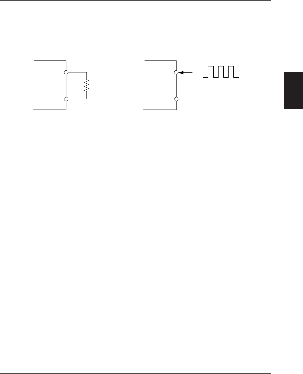
CR Oscillator
S1F76640 has a built-in CR oscillator as the internal oscillator, and an external oscillation resistor ROSC is
connected between the pins OSC1 and OSC2 before operation. (Figure 5.1)
Figure 5-1 CR Oscillator Figure 5-2 External Clock Operation
Note 1 : Since the oscillation frequency varies with wiring capacitance, make the cables between the terminals
OSC1 and OSC2 and R
OSC as short as possible.
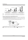
When setting the external resistor R
OSC, find the oscillation frequency fOSC that brings about the maximum effi-
ciency from Figures 6.5.12 and 6.5.13 and find R
OSC suitable for the fOSC from Figure 6.5.1 The relations between
R
OSC and fOSC in Figure 6.5.1 are expressed approximately with the following formula as far as the straight portion
(500kΩ < R
OSC < 2MΩ) is concerned:
R
OSC = A⋅
1
f
OSC
So, the ROSC value can be obtained from this formula.
(Recommended oscillation frequency : 10kHz to 30kHz (R
OSC : 2MΩ to 680kΩ)
When the external clock operates, make the pin OSC2 open as shown in Figure 5.2 and input the 50% duty of the
external clock from the pin OSC1.
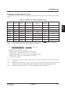
Voltage Conversion Circuits (I) and (II)
The voltage conversion circuits (I) and (II) doubles and triples the input voltage VDD respectively by using clock
generated in the CR oscillator.
In case of 2 times step-up, 2 times step-up output of the input voltage is obtained from the V
O pin when a pump up
capacitor is connected between CAP1+ and CAP1–, CAP2+ and CAP3+ are short-circuited to V
O and a smoothing
capacitor is connected between V
DD and VO outside.
In case of 3 times step-up, 3 V
DD is output from the VO pin when a pump up capacitor is connected between
CAP1+ and CAP1– and between CAP2+ and CAP2– respectively and a smoothing capacitor is connected between
the V
DD and VO pins outside.
In case of 4 times step-up, 4 V
DD is output from the VO pin when a pump up capacitor is connected between
CAP1+ and CAP1–, between CAP2+ and CAP2– and between CAP1+ and CAP3– respectively and a smoothing
capacitor is connected between the V
DD and VO pins outside.
When GND is 0 and V
DD is 5, the relations between the input voltage and the output voltage are as shown in
Figures 5-3, 5-4 and 5-5.
OSC1
OSC2
OSC1
OSC2
Open
External clock
(Note 1)
R
OSC
A : Constant, When GND is 0V and
V
DD is 5V, A is 2.0×10
10
(1/F).)
[ ]