S1F76540 Series
2–16 EPSON S1F70000 Series
Technical Manual
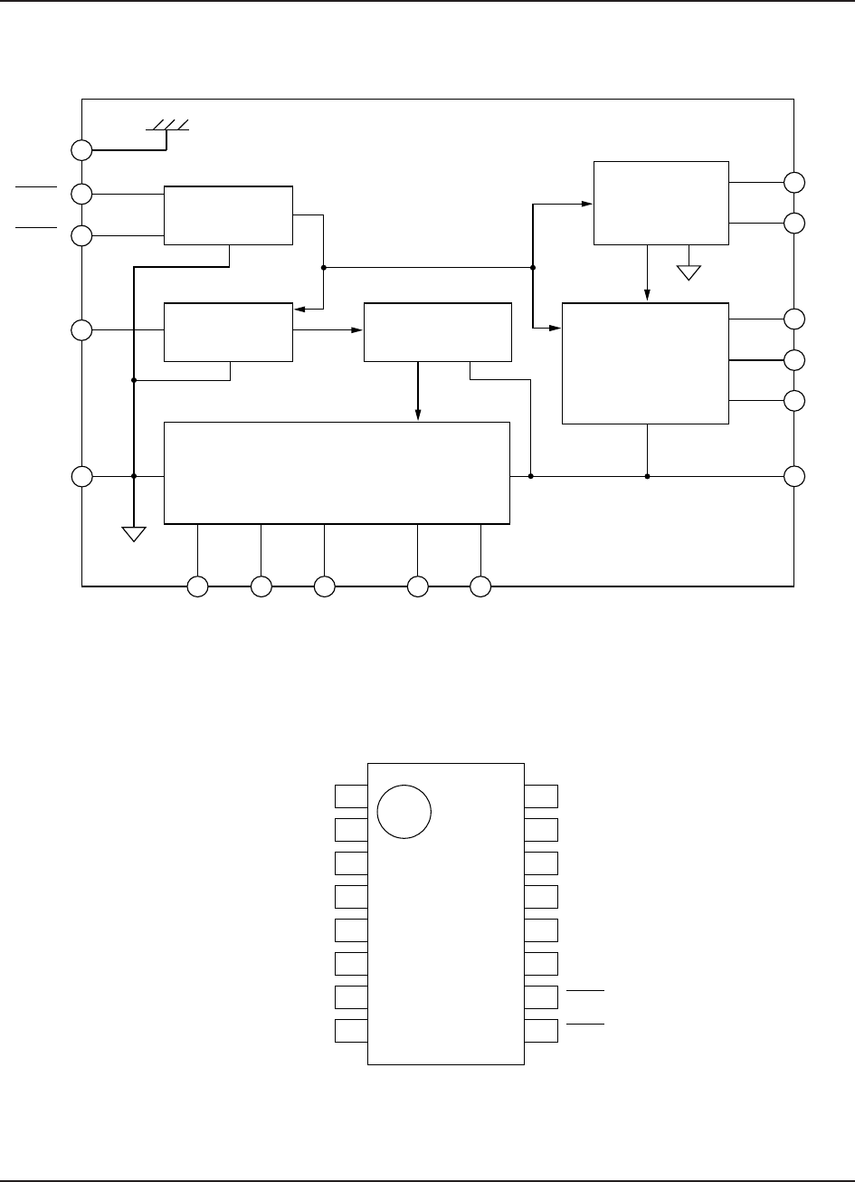
BLOCK DIAGRAM
PIN DESCRIPTIONS
V
DD
Power-off
control circuit
Voltage converter
circuit
Clock
generator
circuit
Booster control
circuit
Voltage
regulation
circuit
Reference
voltage
circuit
C1P C2NC2PC3NC1N
FC
V
I
P
OFF1
P
OFF2
TC1
TC2
V
O
V
RI
RV
V
REG
1
2
3
4
5
6
7
8
V
O
VRI
VREG
RV
V
DD
FC
TC1
TC2
16
15
14
13
12
11
10
9
C2P
C2N
C3N
C1N
C1P
V
I
POFF1
POFF2
Figure 2.1 Block diagram
Figure 2.2 S1F76540M0A0/C0A0 pin assignments


