


SJ100 Inverter
Operations
and Monitoring
4–5
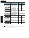
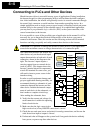
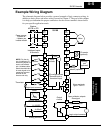
Example Wiring Diagram
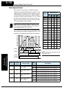
The schematic diagram below provides a general example of logic connector wiring, in
addition to basic power and motor wiring covered in Chapter 2. The goal of this chapter
is to help you determine the proper connections for the various terminals shown below
for your specific application needs.
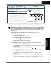
12
11
1
2
3
4
5
6
L
L
H
O
OI
FM
CM2
SJ100
P24
AL1
AL0
AL2
Alarm contacts,
type 1 Form C
Open collector outputs
Analog reference
Power source,
3-phase or
1-phase, per
inverter model
R
(L1)
S
(L2)
T
N(L3)
U
(T1)
V
(T2)
W
(T3)
Motor
Forward
Reverse
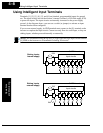
Intelligent inputs,
6 terminals
4–20mA
0–10VDC
NOTE: For the wir-
ing of intelligent I/O
and analog inputs, be
sure to use twisted
pair / shielded cable.
Attach the shield wire
for each signal to its
respective common
terminal at the
inverter end only.
Thermistor
Meter
Analog common
Load
Freq. arrival signal
Run signal
Load
+
–
Logic output common
Input
circuits
[5] configurable as
discrete input or
thermistor input
Logic input common
+
–
24V
+1
+
RB
–
Braking
resistor (optional)
Braking
unit
(optional)
DC reactor
(optional)
Output
circuits
Breaker,
MCCB or GFI