


Intel
®
IXP45X and Intel
®
IXP46X Product Line of Network Processors—General Hardware
Design Considerations
Intel
®
IXP45X and Intel
®
IXP46X Product Line of Network Processors
HDD February 2007
22 Document Number: 305261; Revision: 004
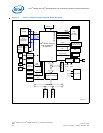
For a complete bit description of Configuration Register 0, see the Intel
®
IXP45X and
Intel
®
IXP46X Product Line of Network Processors Developer’s Manual.
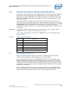
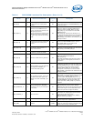
Table 6. Boot/Reset Strapping Configuration (Sheet 1 of 2)
Name Function Description
EX_ADDR[24] (Reserved) (Reserved)
EX_ADDR[23:21]
Intel XScale
®
Processor
Clock Set[2:0]
Allows changing Intel XScale
®
Processor clock speed. This overrides device fuse
settings. However cannot be used to over-clock core speed.
EX_ADDR[20:17] Customer Customer-defined bits. (Might be used for board revision.)
EX_ADDR[16:11] (Reserved) (Reserved)
EX_ADDR[10] IOWAIT_CS0
1 = EX_IOWAIT_N is sampled during the read/write expansion bus cycles for Chip
Select 0.
0 = EX_IOWAIT_N is ignored for read and write cycles to Chip select 0 if
EXP_TIMING_CS0 is configured to Intel mode.
Typically, IOWAIT_CS0 must be pulled down to Vss when attaching a Synchronous
Intel StrataFlash
®
on Chip Select 0 since the default mode for EXP_TIMING_CS0 is
Intel mode and EX_IOWAIT_N is an unknown value for Synchronous Intel
StrataFlash.
If the board does not connect the Synchronous Intel StrataFlash WAIT pin to
EX_WAIT_N (and the board guarantees EX_IOWAIT_N is pulled up), the value of
IOWAIT_CS0 is a don’t-care, since EX_IOWAIT_N will not be asserted.
When EXP_TIMING_CS0 is reconfigure to Intel Synchronous mode during boot-up
(for synchronous Intel chips), the expansion bus controller ignores EX_IOWAIT_N
during read and write cycles since the WAIT functionality is determined from the
EXP_SYNCINTEL_COUNT and EXP_TIMING_CS registers.
EX_ADDR[9] EXP_MEM_DRIVE Refer to table found in EX_ADDR[5].
EX_ADDR[8] USB Clock
Controls the USB clock select.
1 = USB Host/Device clock is generated internally
0 = USB Device clock is generated from GPIO[0].
USB Host clock is generated from GPIO[1]. When generating a spread spectrum
clock on OSC_IN, GPIO[0] can be driven from the system board to generate a
48-MHz clock for the USB Device and GPIO[1] can be driven from the system board
to generate a 60-MHz clock for the USB Host.
EX_ADDR[7] 32_FLASH Refer to table found in EX_ADDR[0]
EX_ADDR[6] EXP_ARB
Configures the Expansion bus arbiter.
0 = External arbiter for Expansion bus.
1 = Expansion bus controller arbiter enabled
EX_ADDR[5] EXP_DRIVE
Expansion bus low/medium/high drive strength. The drive strength depends on
EXP_DRIVE and EXP_MEM_DRIVE configuration bits.
B9. B5
---------------------------------------------------------------------------------------
0 . . 0 Reserved
0 . . 1 Medium Drive
1 . . 0 Low Drive
1 . . 1 High Drive
EX_ADDR[4] PCI_CLK
Sets the clock speed of the PCI Interface
0 = 33 MHz
1 = 66 MHz
EX_ADDR[3] (Reserved) (Reserved). EX_ADDR[3] must not be pulled down during address strapping.