


Intel
®
IXP45X and Intel
®
IXP46X Product Line of Network Processors—Category
Intel
®
IXP45X and Intel
®
IXP46X Product Line of Network Processors
HDD February 2007
76 Document Number: 305261, Revision: 004
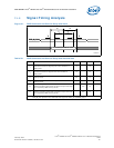
Table 28 provides a list of supported memory configurations that can be implemented
for one or two banks. Notice that depending on the number of devices used, loading of
the driving signals is affected. The most critical signal affected by the loading is the
DDRI_CK (clock output). This signal has a very strict timing requirement defined in the
JEDEC standard, therefore signal integrity of this signal is a must. The following table
shows how to assign the number of devices per clock line for the various configuration.
It also suggest to use a DDR SSTL zero delay clock driver when more than two devices
per clock line are connected. From Table 28, any time the word “driver” appears, it is
meant to let designers know that for that particular configuration, a clock driver is
required. One recommended clock driver can be the Pericom PI6CV855 or a similar
device. The Pericom device is highly used in DIMM memory modules that required to
deliver clocks to many devices in a single module.
The best approach is to minimize the number of devices used to get the target total
memory size required by design.
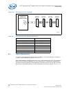
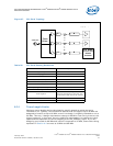
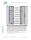
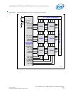
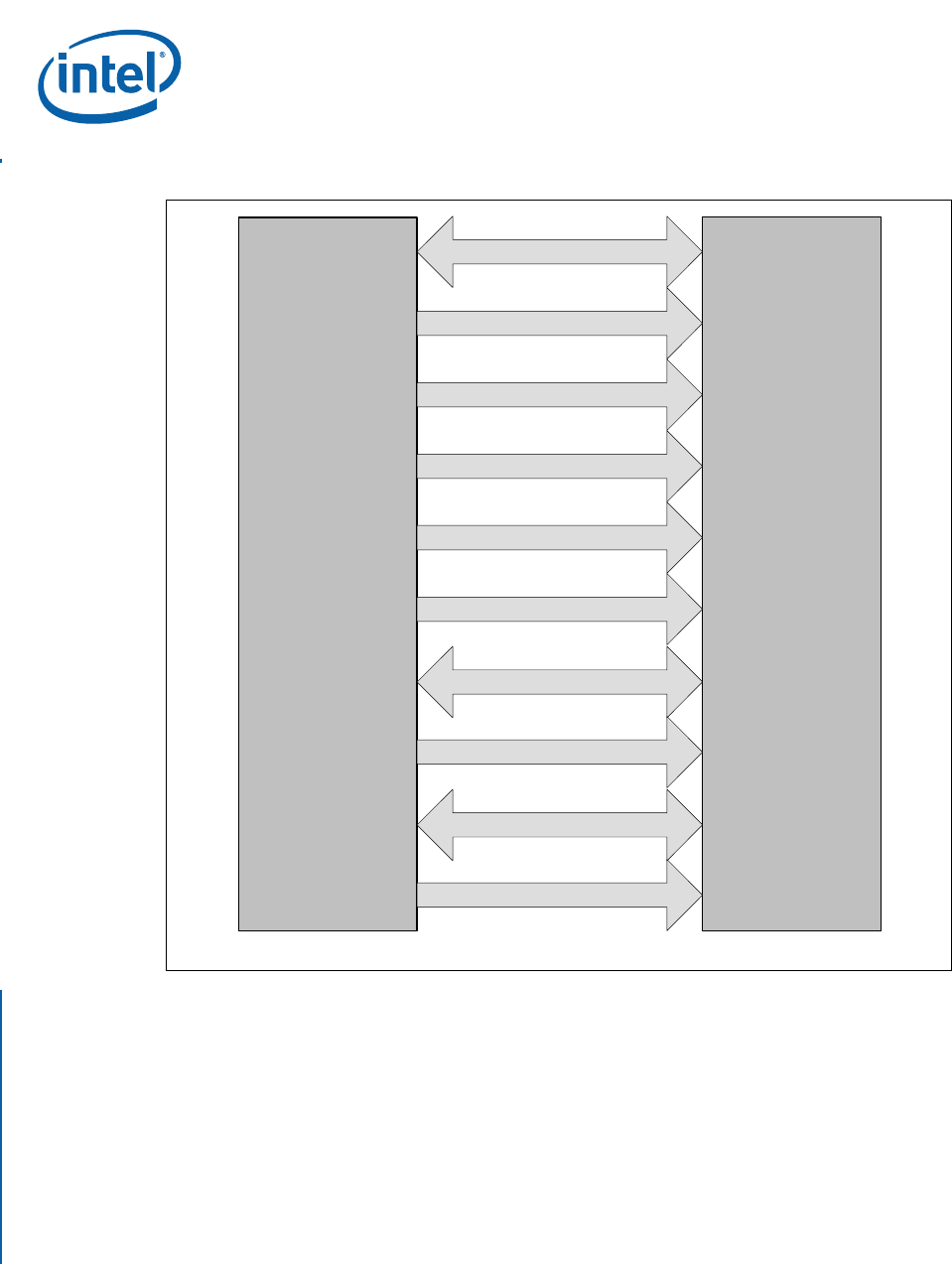
Figure 28. Processor-DDR Interface
DATA[31:0]
ADDRESS[13:0]
CLOCK[2:0], CLOCK#[2:0]
CLOCK ENABLE[1:0]
CHIP SELECT#[1:0]
BANK SELECT[1:0]
DATA MASK[4:0]
WRITE#, RAS#, CAS#
ECC DATA[7:0]
DATA STROBE[4:0]
DDRI_DQ[31:0]
DDRI_MA[13:0]
DDRI_CK[2:0]
DDRI_CK_N[2:0]
DDRI_CKE[1:0]
DDRI_CS_N[1:0]
DDRI_BA[1:0]
DDRI_CB[7:0]
DDRI_DM[4:0]
DDRI_DQS[4:0]
DDRI_WE_N
DDRI_RAS_N
DDRI_CAS_N
DQ[31:0]
A[13:0]
CK[2:0]
CK#[2:0]
CKE[1:0]
CS#[1:0]
BA[1:0]
DQ[7:0]
DM[4:0]
DQS[4:0]
WE#
RAS#
CAS#
DDR SDRAM
Intel
®
Product Line of Network Processors
B3986-001