


Intel
®
IXP45X and Intel
®
IXP46X Product Line of Network Processors—Category
Intel
®
IXP45X and Intel
®
IXP46X Product Line of Network Processors
HDD February 2007
96 Document Number: 305261, Revision: 004
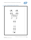
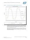
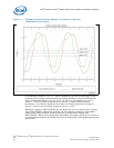
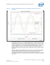
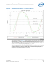
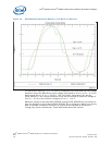
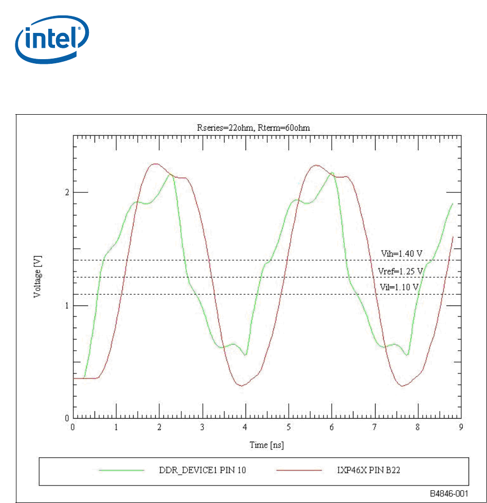
The simulation results in Figure 41 are for the data circuit with a DDR device using
reduced drive strength and shows that the voltage waveform meets the DDR device
input voltage requirements. V
il(max)
of V
ref
– 0.150 or 1.10 V and V
ih(min)
of V
ref
+
0.150 or 1.40 V are easily achieved at the receiver (IXP45X/IXP46X network
processors). The receiver waveform must also not exceed a maximum voltage of
V
in(max)
=2.8 V or the minimum voltage of V
in(min)
=-0.3 V.
Waveform results for DDR_DEVICE2 are not shown as it is not relevant when reading
from DDR_DEVICE1. Due to the symmetry of the topology, waveform results when
reading from DDR_DEVICE2 would be identical to those when reading from
DDR_DEVICE1. When final routing data is available, simulation results for all receivers
are analyzed as variations in routing may result in differences. These differences should
be minimal.
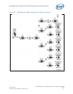
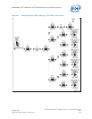
Figure 41. DDR Data Read Simulation Results: Two-Bank x16 Devices
(Reduced Drive Strength)