


Intel
®
IXP45X and Intel
®
IXP46X Product Line of Network Processors
February 2007 HDD
Document Number: 305261; Revision: 004 53
General Hardware Design Considerations—Intel
®
IXP45X and Intel
®
IXP46X Product Line of
Network Processors
3.12.5 Design Notes
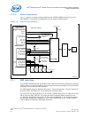
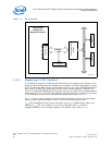
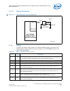
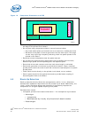
• The IXP45X/IXP46X network processors do not support the 5 V PCI signal interface
by itself. Only the 3.3 V signal interface is supported without signal level
conversion, however, it is possible to interface to 5 V logic when using a voltage
level converter. See Figure 17 for details.
•The PCI Local Bus Specification, Rev. 2.2 requires that the bus is always “parked”,
as some device is always driving the AD lines. There is need to use pull-ups on
these signals. The specification states that the following control lines should be
pulled up:
• The processors’ GPIO pins can be used by PCI devices on PCI slots to request an
interrupt from the processors’ PCI controller.
• PCI_INTA_N is used to request interrupts to external PCI Masters. This signal is an
open collector and requires a pull-up resistor.
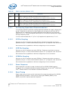
3.13 JTAG Interface
JTAG is the popular name for IEEE standards 1149.1-1990 and 1149.1a-1993, IEEE
Standard Test Access Port and Boundary-Scan Architecture, which provides support
for:
• Board-level boundary-scan connectivity testing
• Connection to software debugging tools through the JTAG interface
• In-system programming of programmable memory and logic devices on the PCB
The interface is controlled through five dedicated test access port (TAP) pins: TDI, TMS,
TCK, nTRST, and TDO, as described in the IEEE 1149.1 standard. The boundary-scan
test-logic elements include the TAP pins, TAP controller, instruction register, boundary-
scan register, bypass register, device identification register, and data-specific registers.
These are described in the Intel
®
IXP45X and Intel
®
IXP46X Product Line of Network
Processors Developer’s Manual.
The IXP45X/IXP46X network processors may be controlled during debug through a
JTAG interface to the processor, the debug tools such as the Macraigor* Raven*, EPI*
Majic*, Wind River Systems* visionPROBE* / visionICE* or various other JTAG tools
plug into the JTAG interface through a connector.
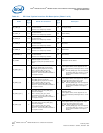
PCI_INTA_N O/D
Connect PCI_INTA_N output from the
Option to one of the GPIO input signals
of the Host. The GPIO signal at the
Host must be configure as an input
interrupt level sensitive.
O/D
Interrupt A
This interrupt is generated from the Option to
one of the GPIO inputs to the Host.
On the Host this signal is not used, it should
be pulled high with a 10-KΩ resistor.
PCI_CLKIN I
Clock must be connected to both
devices. Trace lengths must be
matched. Use point to point clock
distribution.
I Clock input
Table 21. PCI Host/Option Interface Pin Description (Sheet 3 of 3)
Name
Host
Input
Outpu
t
Device-Pin Connection
Option
Input
Outpu
t
Description
— FRAME# — TRDY# — IRDY# — DEVSEL#
—STOP# —SERR# —PERR# —LOCK#
—INTA# —INTB# —INTC# —INTD#