


Intel
®
IXP45X and Intel
®
IXP46X Product Line of Network Processors
February 2007 HDD
Document Number: 305261, Revision: 004 81
DDR-SDRAM—Intel
®
IXP45X and Intel
®
IXP46X Product Line of Network Processors
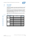
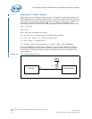
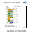
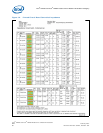
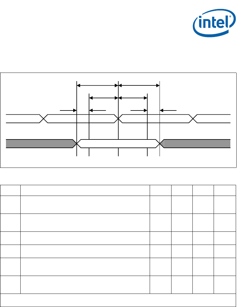
7.1.2 Signal-Timing Analysis
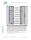
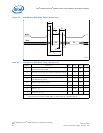
Figure 31. DDR Command and Control Setup and Hold
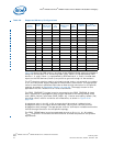
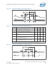
Table 29. DDR Command and Control Setup and Hold Values
Symbol Parameter Min Max Units Notes
T
1
Output of IXP45X/IXP46X network processors valid for
Command and Control signals prior to the transition of
DDR_M_CLK
1.5 ns 1
T
2
Output hold time of IXP45X/IXP46X network processors for
Command and Control signals after the transition of
DDR_M_CLK
1.5 ns 1
T
3
Required Command and Control input setup time at DDR
memory device
0.9 ns 1
T
4
Required Command and Control input hold time at DDR
memory device
0.9 ns 1
T
5
Allowable setup time difference between IXP45X/IXP46X
network processors Command and Control output and setup
time required by DDR memory device
0.6 ns 1
T
6
Allowable hold time difference between IXP45X/IXP46X
network processors Command and Control output and hold
time required by DDR memory device
0.6 ns 1
Notes:
1. DDR_M_CLK represents the combined clock signal for DDRI_CK and DDRI_CK_N.
DDR_M_CLK
Control/Command Valid
T
1
T
2
T
3
T
4
T
6
T
5
B3988-001