


Intel
®
IXP45X and Intel
®
IXP46X Product Line of Network Processors—Category
Intel
®
IXP45X and Intel
®
IXP46X Product Line of Network Processors
HDD February 2007
88 Document Number: 305261, Revision: 004
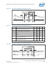
In addition to any trace length differentials which must be considered between signal
groups, differences in the package length between signals should be considered when
determining the total propagation delay of the signals. When using the IBIS model for
signal analysis, package characteristics are included in the simulation results.
7.1.6 Resistive Compensation Register (Rcomp)
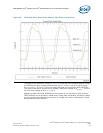
Critical signals such as the differential clock drivers used for driving clock out to
memory devices is very critical. The JEDEC standard has a very critical requirement for
the crossing of the differential clock signals which required proper termination and
drive strength of the signals. Therefore, in order to comply with this requirement, two
recommendations have been made.
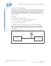
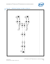
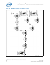
• Use Thevenin termination as shown in Figure 37. It is important that the series
termination and impedance matching is strictly follow.
• Configuration of the Rcomp circuit.
The steps to follow and the order in which they need to occur to configure Rcomp are
described in section “DDRI SDRAM Initialization” of the Intel
®
IXP45X and Intel
®
IXP46X Product Line of Network Processors Developer’s Manual. Here is a recap of the
two registers that are required to be overwritten with the new value:
• Override default value of register DDR_RCOMP_CSR3 with 0x0000 1000Hex
• Override default value of register DDR_DRIVE3 with 0x0002 08F0Hex
Note that this configuration only affects the SDRAM differential clock driver for all three
outputs DDRI_CK[2:0] and DDRI_CK_N[2:0].
Refer to the Intel
®
IXP45X and Intel
®
IXP46X Product Line of Network Processors
Developer’s Manual for the complete sequence of steps to follow to configure the
SDRAM DDRI memory module.
Note that when simulating, the IBIS model representation of signals DDRI_CK[2:0] and
DDRI_CK_N[2:0] has been created for the new Rcomp settings described in this
section.
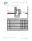
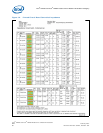
7.1.7 Routing Guidelines
7.1.7.1 Clock Group
The clock signal group includes the differential clock pairs DDRI_CK[2:0] and
DDRI_CK_N[2:0].
Here are some tips on how to route the differential clock pairs:
• Ensure that DDR clocks are routed on a single internal layers, except for pin
escapes.
• A ground plane must be adjacent to the layer where the signals are routed.
• Minimize the number of vias used, but ensure that the same number of vias are
used in the positive and negative trace.
• It is recommended that pin escape vias be located directly adjacent to the ball pads
on all clocks.
• Traces must be routed for differential mode impedance of 120 Ω.
• Surface layer routing should be minimized (top or bottom layers).
• It is recommended to perform pre- and post-layout simulation.
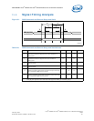
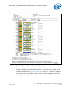
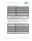
Table 34 provides routing guidelines for signals within this group.