


1999 May 10 14
Philips Semiconductors Preliminary specification
Universal Serial Bus (USB) CODEC UDA1325
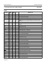
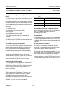
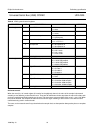
Table 6 Selection of data transfer type
Data bits 7 to 2 represent a 6-bit device address, with bit 7 being the MSB and bit 2 the LSB. The address of the ADAC
is 000101 (bits 7 to 2). In the event that the ADAC receives a different address, it will deselect its microcontroller interface
logic.
D
ATA TRANSFER MODE
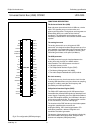
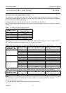
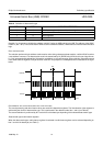
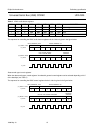
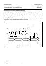
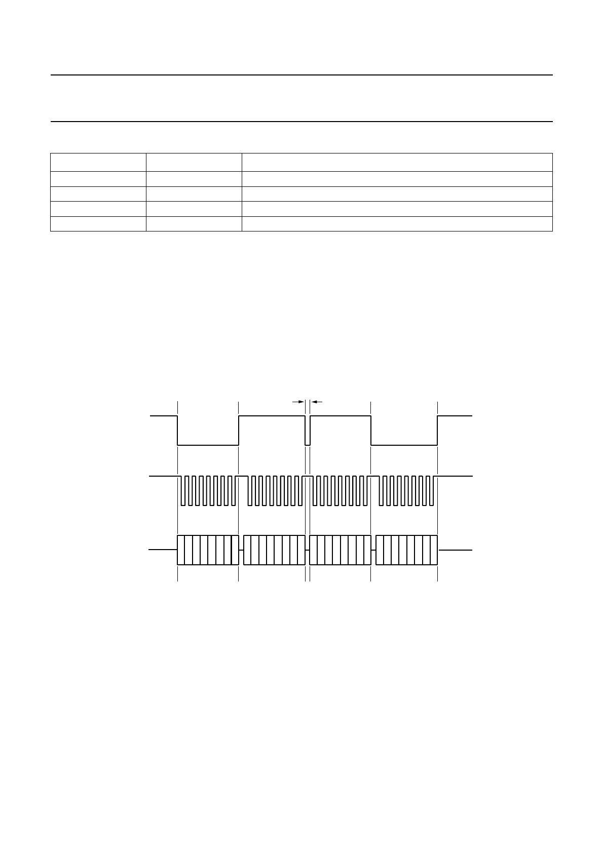
The selection preformed in the address mode remains active during subsequent data transfers, until the ADAC receives
a new address command. The data transfer mode is characterized by L3_MODE being HIGH and a burst of 8 pulses on
L3_CLK, accompanied by 8 data bits. All transfers are bitwise, i.e. they are based on groups of 8 bits. Data will be stored
in the ADAC after the eight bit of a byte has been received. The principle of a multibyte transfer is illustrated in the figure
below.
P
ROGRAMMING THE SOUND PROCESSING AND OTHER FEATURES
The sound processing and other feature values are stored in independent registers. The first selection of the registers is
achieved by the choice of data transfer type. This is performed in the address mode, bits 1 and 0 (see Table 6).
The second selection is performed by bit 7 and/or bit 6 of the data byte depending of the selected data transfer type.
Data transfer type ‘audio feature registers’
When the data transfer type ‘audio feature registers’ is selected 4 audio feature registers can be selected depending on
bits 7 and 6 of the data byte (see Table 7).
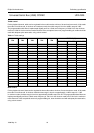
BIT1 BIT0 DATA TRANSFER TYPE
0 0 audio feature registers (volume left, volume right, bass and treble)
0 1 not used
1 0 control registers
1 1 not used
n
dbook, full pagewidth
t
halt
address
L3DATA
L3CLOCK
L3MODE
addressdata byte #1 data byte #2
MGD018