


1999 May 10 40
Philips Semiconductors Preliminary specification
Universal Serial Bus (USB) CODEC UDA1325
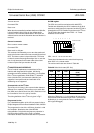
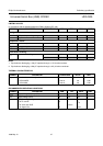
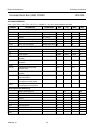
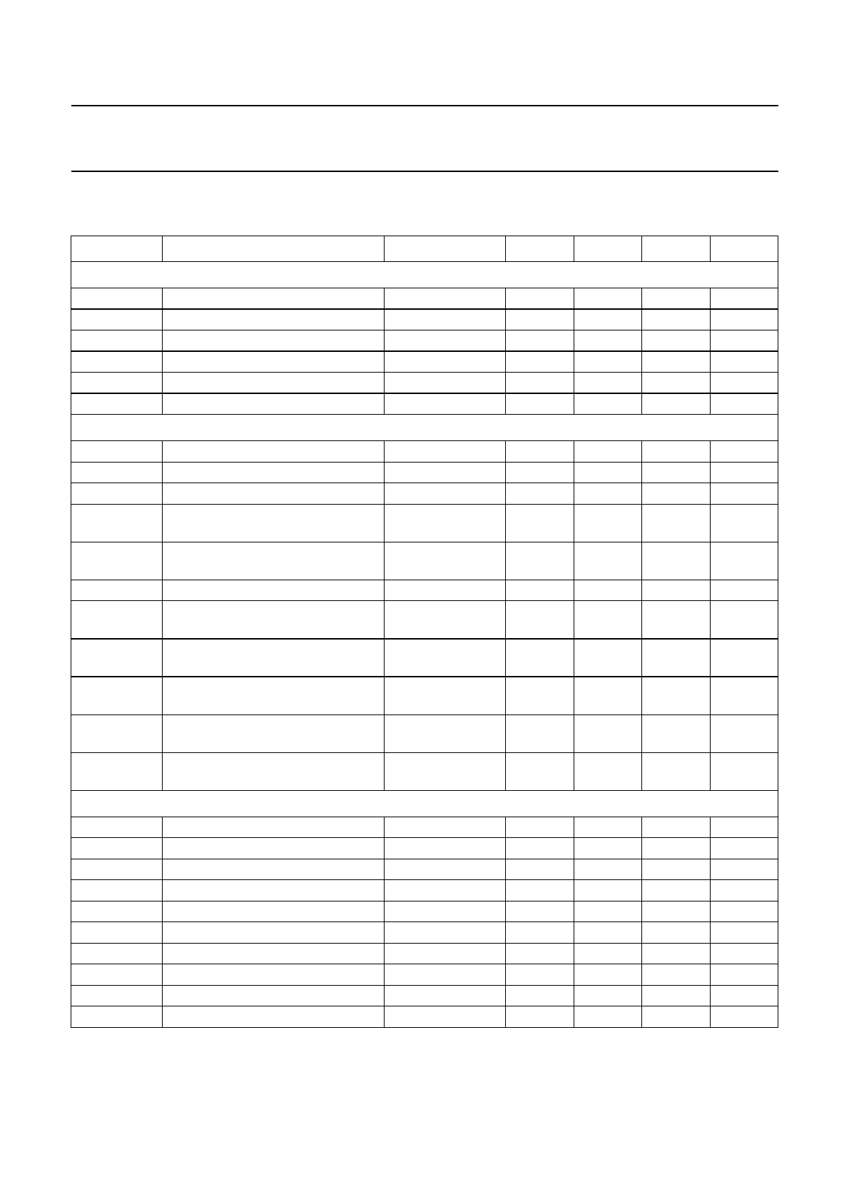
AC CHARACTERISTICS
V
DDE
= 5.0 V; V
DDI
= 3.3 V; T
amb
=25°C; f
osc
= 48 MHz; f
s
= 44.1 kHz; unless otherwise specified.
SYMBOL PARAMETER CONDITIONS MIN. TYP. MAX. UNIT
Driver characteristics D+ and D− (full-speed mode)
f
o(s)
audio sample output frequency 5 − 55 kHz
t
r
rise time C
L
=50pF 4 − 20 ns
t
f
fall time C
L
=50pF 4 − 20 ns
t
rf(m)
rise/fall time matching (t
r
/t
f
)90−110 %
V
cr
output signal crossover voltage 1.3 − 2.0 V
R
o(drive)
driver output resistance steady-state drive 28 − 43 Ω
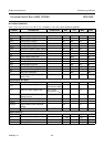
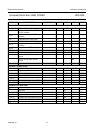
Data source timings D+ and D− (full-speed mode)
f
i(s)
audio sample input frequency 5 − 55 kHz
f
fs(D)
full speed data rate 11.97 12.00 12.03 Mbits/s
t
fr(D)
frame interval 0.9995 1.0000 1.0005 ms
t
J1(diff)
source differential jitter to next
transition
−3.5 0.0 +3.5 ns
t
J2(diff)
source differential jitter for paired
transitions
−4.0 0.0 +4.0 ns
t
W(EOP)
source end of packet width 160 − 175 ns
t
EOP(diff)
differential to end of packet
transition skew
−2.0 − +5.0 ns
t
JR1
receiver data jitter tolerance to next
transition
−18.5 0.0 +18.5 ns
t
JR2
receiver data jitter tolerance for
paired transitions
−9.0 0.0 +9.0 ns
t
EOPR1
end of packet width at receiver
must reject as end of packet
40 −−ns
t
EOPR2
end of packet width at receiver
must accept as end of packet
82 −−ns
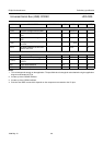
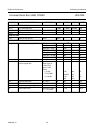
Serial input/output data timing
f
s
system clock frequency − 12 − MHz
f
i(WS)
word selection input frequency 5 − 55 kHz
t
r
rise time −−20 ns
t
f
fall time −−20 ns
t
BCK(H)
bit clock HIGH time 55 −−ns
t
BCK(L)
bit clock LOW time 55 −−ns
t
s;DAT
data set-up time 10 −−ns
t
h;DAT
data hold time 20 −−ns
t
s;WS
word selection set-up time 20 −−ns
t
h;WS
word selection hold time 10 −−ns