


1999 May 10 6
Philips Semiconductors Preliminary specification
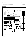
Universal Serial Bus (USB) CODEC UDA1325
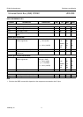
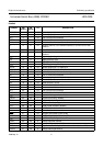
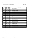
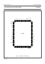
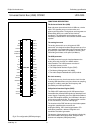
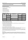
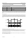
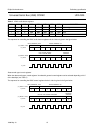
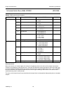
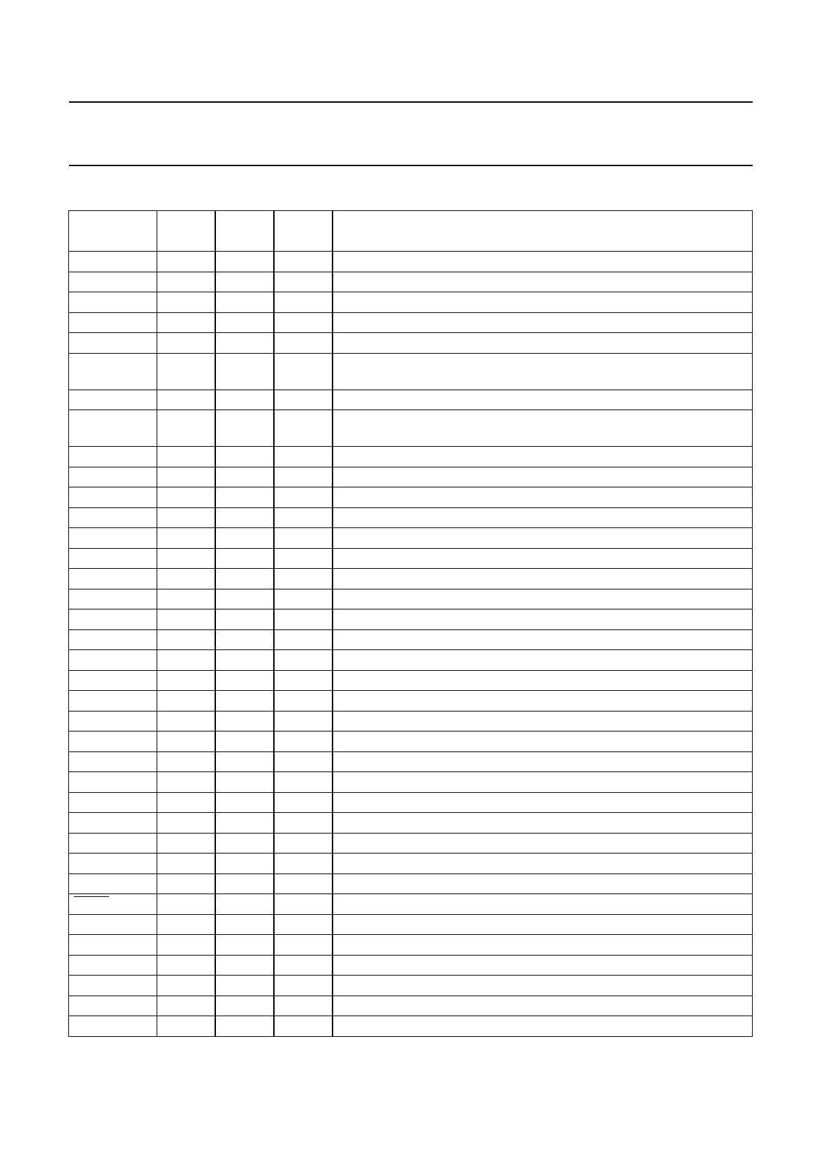
PINNING
SYMBOL
PIN
QFP64
PIN
SDIP42
I/O DESCRIPTION
GP3/WSO 1 5 I/O general purpose pin 3 or word select output
GP4/BCKO 2 6 I/O general purpose pin 4 or bit clock output
P0.5 3 − I/O Port 0.5 of the microcontroller
SHTCB 4 7 I shift clock of the test control block (active HIGH)
P0.6 5 − I/O Port 0.6 of the microcontroller
D− 6 8 I/O negative data line of the differential data bus, conforms to the USB
standard
P0.7 7 − I/O Port 0.7 of the microcontroller
D+ 8 9 I/O positive data line of the differential data bus, conforms to the USB
standard
V
DDI
910−digital supply voltage for core
V
SSI
10 11 − digital ground for core
V
SSE
11 12 − digital ground for I/O pads
V
DDE
12 13 − digital supply voltage for I/O pads
GP1/DI 13 14 I/O general purpose pin 1 or data input
P2.0 14 − I/O Port 2.0 of the microcontroller
GP5/WSI 15 15 I/O general purpose pin 5 or word select input
P2.1 16 − I/O Port 2.1 of the microcontroller
GP0/BCKI 17 16 I/O general purpose pin 0 or bit clock input
P2.2 18 − I/O Port 2.2 of the microcontroller
SCL 19 17 I/O serial clock line I
2
C-bus
P2.3 20 − I/O Port 2.3 of the microcontroller
SDA 21 18 I/O serial data line I
2
C-bus
P2.4 22 − I/O Port 2.4 of the microcontroller
P2.5 23 − I/O Port 2.5 of the microcontroller
V
SSX
24 19 − crystal oscillator ground (48 MHz)
XTAL1b 25 20 I crystal input (analog; 48 MHz)
XTAL2b 26 21 O crystal output (analog; 48 MHz)
CLK 27 − O 48 MHz clock output signal
V
DDX
28 22 − supply crystal oscillator (48 MHz)
P2.6 29 − I/O Port 2.6 of the microcontroller
P2.7 30 − I/O Port 2.7 of the microcontroller
PSEN 31 − I/O program store enable (active LOW)
V
DDO
32 23 − supply voltage for operational amplifier
V
SSO
33 24 − operational amplifier ground
VOUTL 34 25 O voltage output left channel
TC 35 26 I test control input (active HIGH)
RTCB 36 27 I asynchronous reset input of the test control block (active HIGH)
VOUTR 37 28 O voltage output right channel