


1999 May 10 39
Philips Semiconductors Preliminary specification
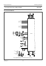
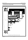
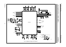
Universal Serial Bus (USB) CODEC UDA1325
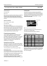
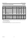
Notes
1. This value depends strongly on the application. The specified value is the typical value obtained using the application
diagram as illustrated in Fig.8.
2. At start-up of the OSCAD oscillator.
3. At start-up of the OSC48 oscillator.
4. Exclusive the IDDE current which depends on the components connected to the I/O pins.
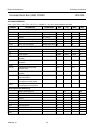
PGA and ADC
V
ref(AD)
reference voltage PGA and ADC − 0.5V
DDA2
− V
V
ref(ADC)(pos)
positive reference voltage of the
ADC
− V
DDA2
− V
V
ref(ADC)(neg)
negative reference voltage of the
ADC
− 0.0 − V
V
I(PGA)
DC input voltage VINL and VINR of
the PGA
− 0.5V
DDA2
− V
R
I(PGA)
DC input resistance at VINL and
VINR of the PGA
− 12.5 − kΩ
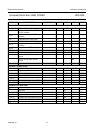
Filter stream DAC
V
ref(DA)
reference voltage DAC − 0.5V
DDA1
− V
V
O(CM)
common mode output voltage − 0.5V
DDA1
− V
R
O(VOUT)
output resistance at VOUTL and
VOUTR
− 11 −Ω
R
O(L)
output load resistance 2.0 −−kΩ
C
O(L)
output load capacitance −−50 pF
SYMBOL PARAMETER CONDITIONS MIN. TYP. MAX. UNIT