


1999 May 10 43
Philips Semiconductors Preliminary specification
Universal Serial Bus (USB) CODEC UDA1325
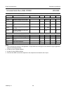
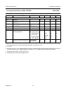
Notes
1. Strongly depends on the external decoupling capacitor connected to V
ref(DA)
.
2. C
ref
in µF.
3. Although a level of 1.414 V (RMS) would be required to optimal drive the ADC in this gain setting, this level can not
be used. Due to the 3.3 V supply voltage input, signals of 1.17 V (RMS) and higher will result in clipping.
4. Measured with the APLL as ADC clock source.
5. Measured with I
2
S-bus input as digital source.
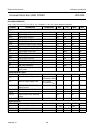
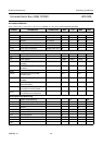
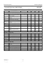
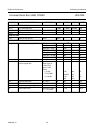
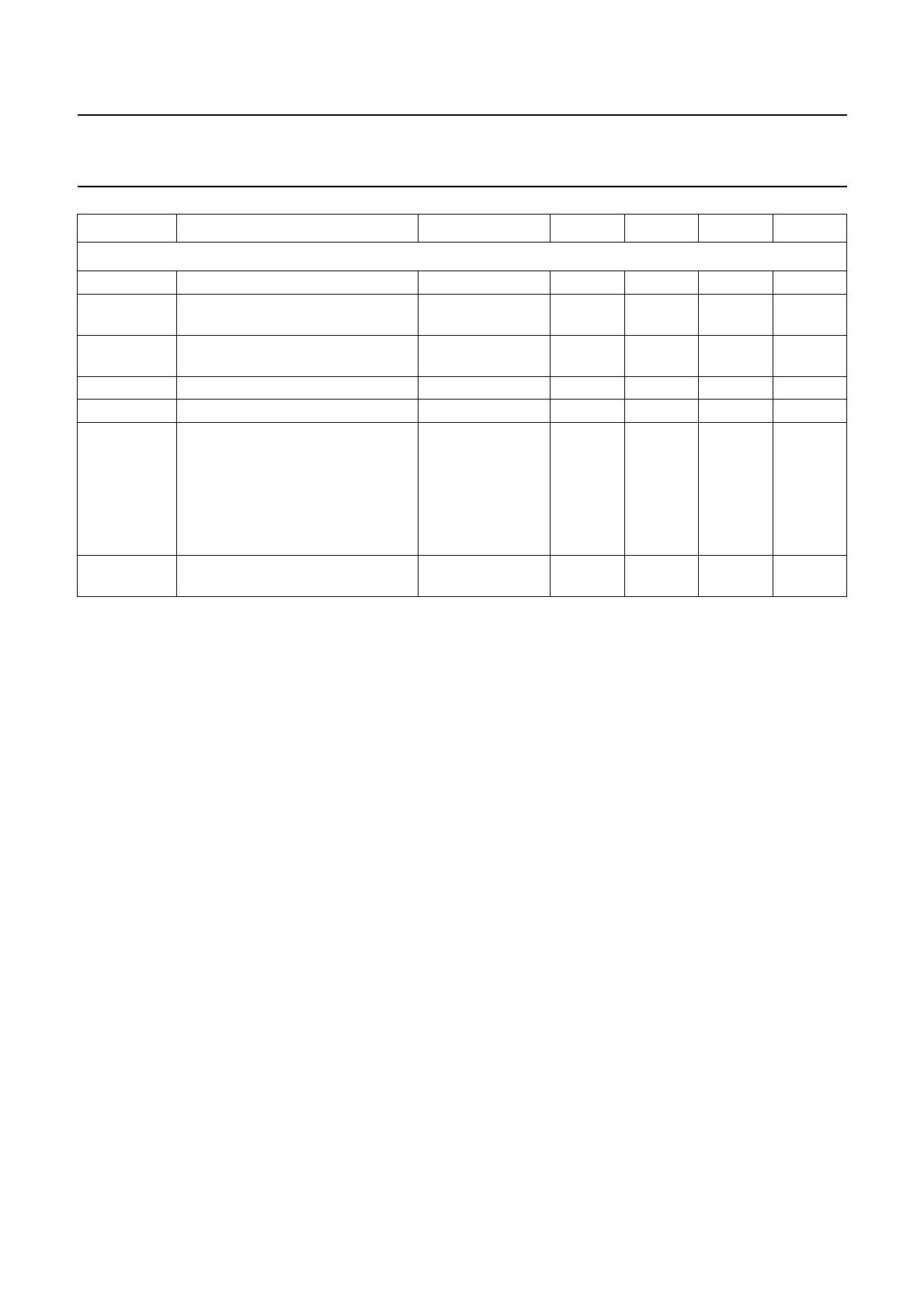
Filter stream DAC
RES resolution 16 −−bits
V
o(FS)(rms)
full-scale output voltage
(RMS value)
V
DD
= 3.3 V − 0.66 − V
SVRR supply voltage ripple rejection at
V
DDA
and V
DDO
f
ripple
= 1 kHz
V
ripple(p-p)
= 0.1 V
− 60 − dB
∆V
o
channel unbalance maximum volume − 0.03 − dB
α
ct
crosstalk between channels R
L
=5kΩ−95 − dB
(THD + N)/S total harmonic distortion plus
noise-to-signal ratio
f
s
= 44.1 kHz;
R
L
=5kΩ; note 5
at input signal of
1 kHz (0 dB)
−−90 −80 dB
− 0.0032 0.01 %
at input signal of
1 kHz (−60 dB)
−−30 −20 dB
− 3.2 10 %
S/N signal-to-noise ratio at bipolar zero A-weighting at
code 0000H
90 95 − dB
SYMBOL PARAMETER CONDITIONS MIN. TYP. MAX. UNIT