


1999 May 10 24
Philips Semiconductors Preliminary specification
Universal Serial Bus (USB) CODEC UDA1325
MEMORY AND REGISTER SPACE 80C51
Overview registers
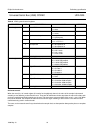
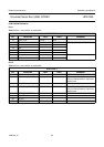
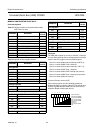
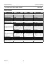
Table 15 Register location and recommended values
after Power-on reset
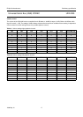
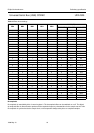
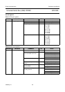
Table 16 Special function register location
ADDRESS REGISTER
RESET
VALUE
0800h PGA gain 09
0801h ADIF control 5C
1000h clock shop settings 00
1001h reset control and APLL settings 00
1002h IO selection register 01
1003h power control 00
2000h ASR settings 8B
4000h data register PSIE
4001h command register PSIE
ADDRESS REGISTER
RESET
VALUE
CPU registers
81h SP
82h DPL
83h DPH
D0h PSW
E0h ACC
F0h B
Interrupt registers
A8h IE 00h
B8h IP 00h
Timer 0 and Timer 1 registers
88h T01CON 00h
89h T01MOD 00h
8Ah T0L 00h
8Bh T1L 00h
8Ch T0h 00h
8Dh T1h 00h
PCON registers
87h PCON 00h
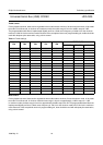
Interrupts
The UDA1325 supports up to five (of maximal 7) interrupt
sources. Each interrupt source corresponds to an interrupt
vector in the CPU program memory address space:
Source 0: vector 0003h external interrupt 0 (INT0_N)
Source 1: vector 000Bh Timer 0 interrupt
Source 2: vector 0013h external interrupt 1 (INT1_N)
Source 3: vector 001Bh Timer 1 interrupt
Source 4: vector 0023h UART interrupt (not present)
Source 5: vector 002Bh Timer 2 interrupt (not present)
Source 6: vector 0033h I
2
C interrupt.
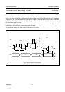
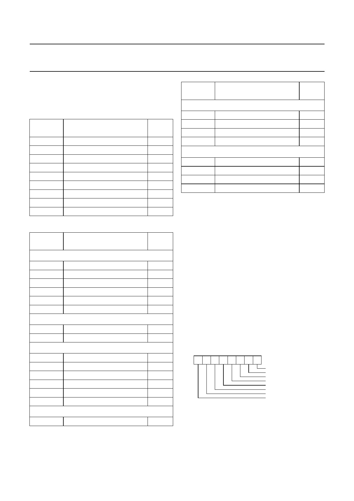
I
NTERRUPT ENABLE REGISTER (IE)
Each interrupt source can be individually enabled or
disabled by setting or clearing a bit in IE. This register also
contains a global interrupt enable bit (EA) which can be
cleared to disable all interrupts at once.
Port registers
80h P0 FFh
90h P1 FFh
A0h P2 FFh
B0h P3 FFh
I
2
C registers (SIO1 registers)
D8h S1CON 00h
D9h S1STA
DAh S1DAT
DBh S1ADR
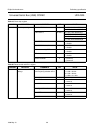
ADDRESS REGISTER
RESET
VALUE
0 0 0 0 0 0 0 0
EX0 (vector 0003h))
ET0 (vector 000Bh))
EX1 (vector 0013h)
ET1 (vector 001Bh)
ES0 (n.a.)
ET2 (n.a.)
ES1 (vector 0033h)
EA
76543210
Power On Value