APPLICATION
2.2 Interrupts
2-14
4513/4514 Group User’s Manual
(2) Interrupt control register V1
Interrupt enable bits of external 0, external 1, timer 1 and timer 2 are assigned to register V1.
Set the contents of this register through register A with the TV1A instruction.
In addition, the TAV1 instruction can be used to transfer the contents of register V1 to register A.
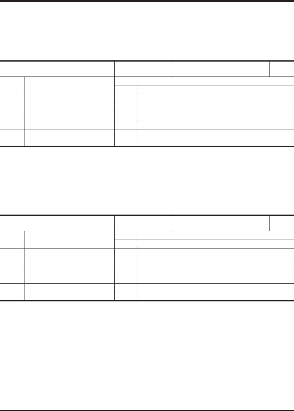
Table 2.2.1 shows the interrupt control register V1.
Table 2.2.1 Interrupt control register V1
Interrupt control register V1 at reset : 00002 at RAM back-up : 00002
R/W
Interrupt disabled (SNZT2 instruction is valid)
Interrupt enabled (SNZT2 instruction is invalid)
Interrupt disabled (SNZT1 instruction is valid)
Interrupt enabled (SNZT1 instruction is invalid)
Interrupt disabled (SNZ1 instruction is valid)
Interrupt enabled (SNZ1 instruction is invalid)
Interrupt disabled (SNZ0 instruction is valid)
Interrupt enabled (SNZ0 instruction is invalid)
Timer 2 interrupt enable bit
Timer 1 interrupt enable bit
External 1 interrupt enable bit
External 0 interrupt enable bit
V13
V12
V11
V10
0
1
0
1
0
1
0
1
Note: “R” represents read enabled, and “W” represents write enabled.
(4) Interrupt request flag
The activated condition for each interrupt is examined. Each interrupt request flag is set to “1” when
the activated condition is satisfied, even if the interrupt is disabled by the INTE flag or its interrupt
enable bit.
Each interrupt request flag is cleared to “0” when either;
•an interrupt occurs, or
•the next instruction is skipped with a skip instruction.
Interrupt control register V2 at reset : 00002 at RAM back-up : 00002
R/W
Interrupt disabled (SNZSI instruction is valid)
Interrupt enabled (SNZSI instruction is invalid)
Interrupt disabled (SNZAD instruction is valid)
Interrupt enabled (SNZAD instruction is invalid)
Interrupt disabled (SNZT4 instruction is valid)
Interrupt enabled (SNZT4 instruction is invalid)
Interrupt disabled (SNZT3 instruction is valid)
Interrupt enabled (SNZT3 instruction is invalid)
Serial I/O interrupt enable bit
A-D interrupt enable bit
Timer 4 interrupt enable bit
Timer 3 interrupt enable bit
V23
V22
V21
V20
0
1
0
1
0
1
0
1
Note: “R” represents read enabled, and “W” represents write enabled.
(3) Interrupt control register V2
Interrupt enable bits of timer 3, timer 4, A-D, and serial I/O are assigned to register V2.
Set the contents of this register through register A with the TV2A instruction.
In addition, the TAV2 instruction can be used to transfer the contents of register V2 to register A.
Table 2.2.2 shows the interrupt control register V2.
Table 2.2.2 Interrupt control register V2


