APPLICATION
2.5 A-D converter
2-53
4513/4514 Group User’s Manual
(5) A-D converter is used at the comparator mode
The analog input voltage is higher than the comparison voltage as a result of comparison, the
contents of ADF flag retains “0,” not set to “1.”
In this case, the A-D interrupt does not occur even when the usage of the A-D interrupt is enabled.
Accordingly, consider the time until the comparator operation is completed, and examine the state
of ADF flag by software. The comparator operation is completed after 8 machine cycles.
(6) Analog input pins
Even when P40/AIN4–P43/AIN7 are set to pins for analog input, they continue to function as P40–P43
I/O. Accordingly, when any of them are used as I/O port P4 and others are used as analog input pins,
make sure to set the outputs of pins that are set for analog input to “1.” Also, the port input function
of the pin functions as an analog input is undefined.
(7) TALA instruction
When the TALA instruction is executed, the low-order 2 bits of register AD is transferred to the high-
order 2 bits of register A, and simultaneously, the low-order 2 bits of register A is “0.”
(8) Recommended operating conditions when using A-D converter
The recommended operating conditions of supply voltage and system clock frequency when using A-
D converter are different from those when not using A-D converter.
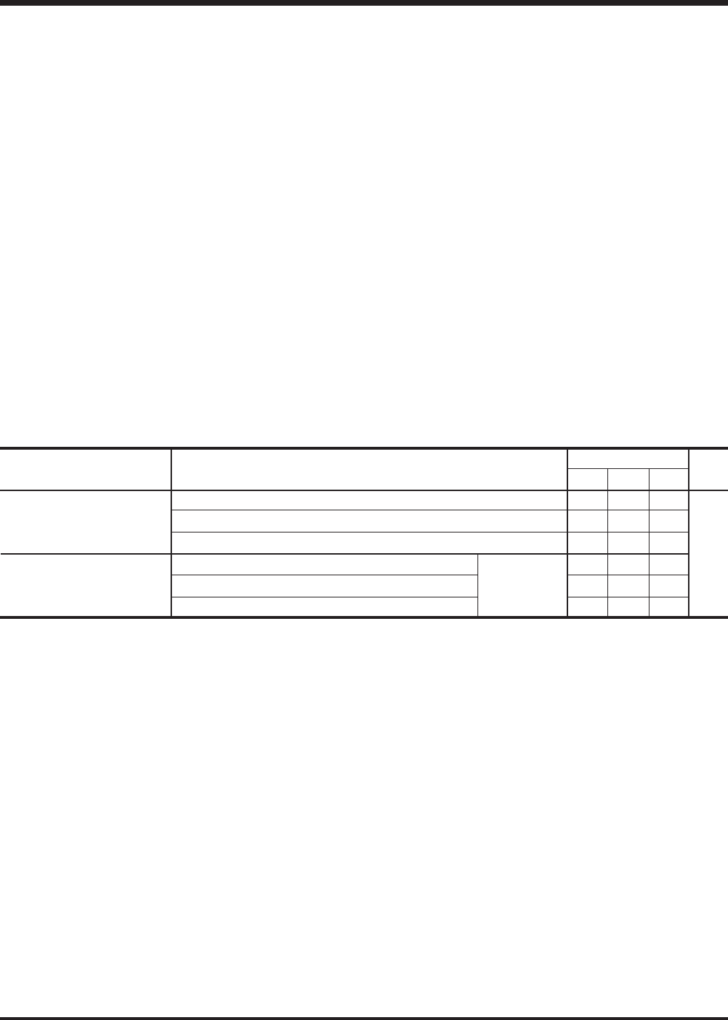
Table 2.5.3 shows the recommended operating conditions when using A-D converter.
Table 2.5.3 Recommended operating conditions (when using A-D converter)
Parameter
System clock frequency
(at ceramic resonance)
System clock frequency
(at external clock input)
Condition
VDD = 4.5 V to 5.5 V (high-speed mode)
VDD = 4.0 V to 5.5 V (high-speed mode)
VDD = 2.7 V to 5.5 V (middle-speed mode)
VDD = 4.5 V to 5.5 V (high-speed mode)
VDD = 4.0 V to 5.5 V (high-speed mode)
VDD = 2.7 V to 5.5 V (middle-speed mode)
Limits
Min.
0.4
0.4
0.4
0.4
0.4
0.4
Max.
4.2
2.0
4.2
3.0
1.0
3.0
Unit
MHz
Typ.
Duty
40 % to 60 %


