4513/4514 Group User’s Manual
APPENDIX
3-25
3.4 Notes on noise
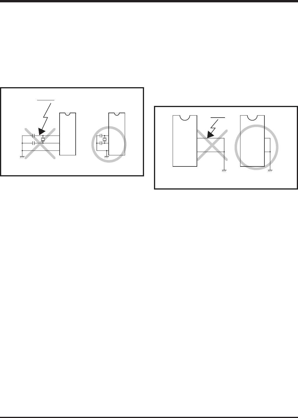
(3) Wiring for clock input/output pins
• Make the length of wiring which is connected
to clock I/O pins as short as possible.
• Make the length of wiring across the
grounding lead of a capacitor which is
connected to an oscillator and the VSS pin
of a microcomputer as short as possible.
• Separate the VSS pattern only for oscillation
from other VSS patterns.
Fig. 3.4.3 Wiring for clock I/O pins
● Reason
If noise enters clock I/O pins, clock
waveforms may be deformed. This may
cause a program failure or program runaway.
Also, if a potential difference is caused by
the noise between the VSS level of a
microcomputer and the VSS level of an
oscillator, the correct clock will not be input
in the microcomputer.
Fig. 3.4.4 Wiring for CNVSS pin
Noise
XIN
XOUT
VSS
XIN
XOUT
VSS
N.G.
O.K.
Noise
CNVSS
VSS
CNVSS
VSS
N.G.
O.K.
(4) Wiring to CNVSS pin
Connect the CNVSS pin to the VSS pin with
the shortest possible wiring.
● Reason
The operation mode of a microcomputer is
influenced by a potential at the CNVSS pin.
If a potential difference is caused by the
noise between pins CNVSS and VSS, the
operation mode may become unstable. This
may cause a microcomputer malfunction or
a program runaway.


