1-46
HARDWARE
4513/4514 Group User’s Manual
FUNCTION BLOCK OPERATIONS
(15) Notes for the use of A-D conversion 2
Do not change the operating mode (both A-D conversion mode and
comparator mode) of A-D converter with bit 3 of register Q2 while
A-D converter is operating.
When the operating mode of A-D converter is changed from the
comparator mode to A-D conversion mode with the bit 3 of register
Q2, note the following;
• Clear bit 2 of register V2 to “0” to change the operating mode of
the A-D converter from the comparator mode to A-D conversion
mode with the bit 3 of register Q2.
• The A-D conversion completion flag (ADF) may be set when the
operating mode of the A-D converter is changed from the com-
parator mode to the A-D conversion mode. Accordingly, set a
value to register Q2, and execute the SNZAD instruction to clear
the ADF flag.
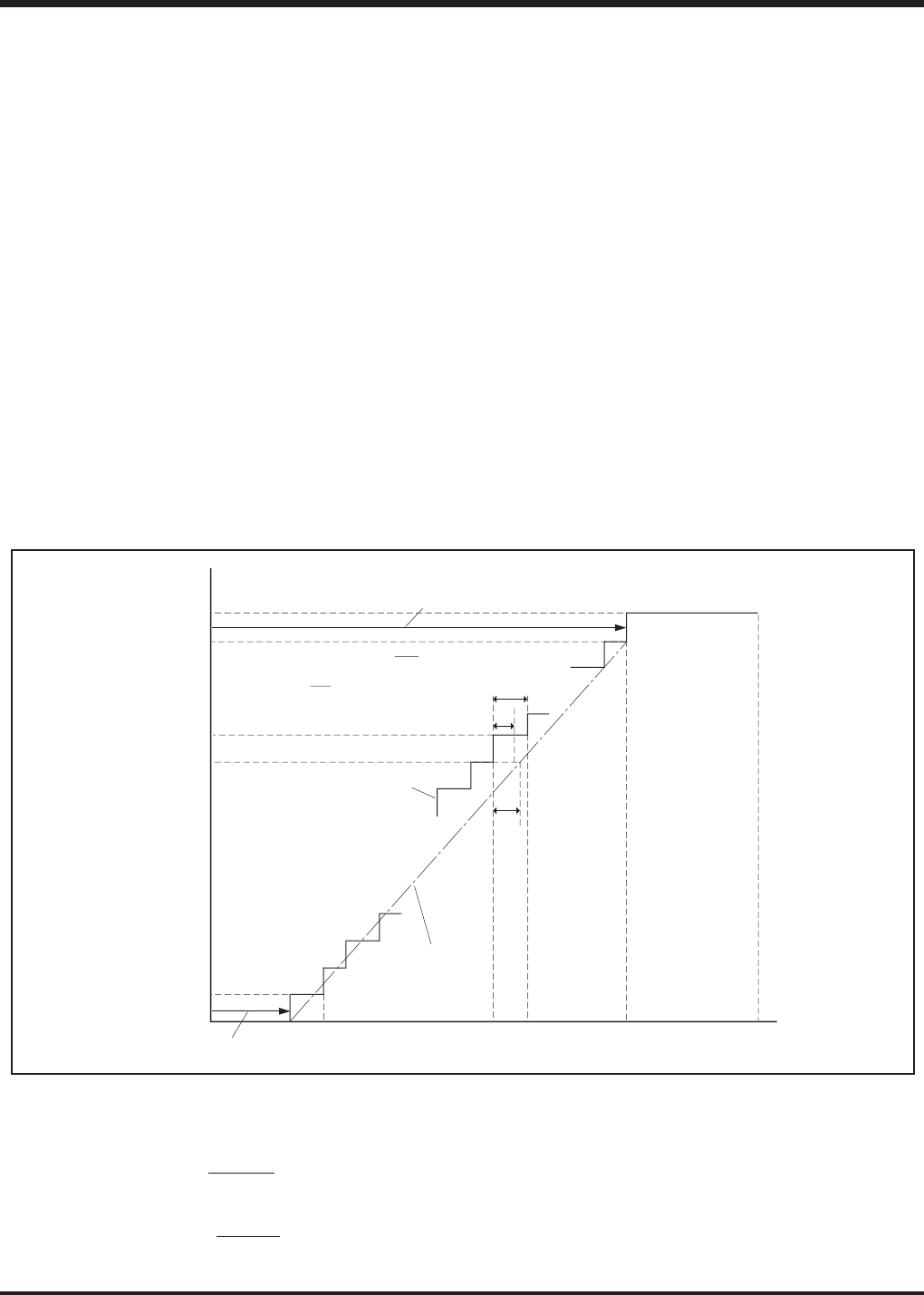
(16) Definition of A-D converter accuracy
The A-D conversion accuracy is defined below (refer to Figure 30).
• Relative accuracy
➀ Zero transition voltage (V0T)
This means an analog input voltage when the actual A-D con-
version output data changes from “0” to “1.”
➁ Full-scale transition voltage (VFST)
This means an analog input voltage when the actual A-D con-
version output data changes from “1023” to ”1022.”
➂ Linearity error
This means a deviation from the line between V0T and VFST of
a converted value between V0T and VFST.
➃ Differential non-linearity error
This means a deviation from the input potential difference re-
quired to change a converter value between V0T and VFST by 1
LSB at the relative accuracy.
• Absolute accuracy
This means a deviation from the ideal characteristics between 0
to VDD of actual A-D conversion characteristics.
Fig. 30 Definition of A-D conversion accuracy
Vn: Analog input voltage when the output data changes from “n” to “n+1” (n = 0 to 1022)
• 1LSB at relative accuracy → (V)
• 1LSB at absolute accuracy → (V)
VFST–V0T
1022
VDD
1024
V
DD
V
1022
V
n
V
1
V
0
V
n+1
n+1
n
1022
1023
1
0
b
a
c
Output data
Differential non-linearity error =
Linearity error =
[LSB]
c
a
b–a
a
[LSB]
Actual A-D conversion
characteristics
a: 1LSB by relative accuracy
b: V
n+1
–V
n
c: Difference between ideal V
n
and actual V
n
Zero transition voltage (V
0T
)
Analog voltage
Full-scale transition voltage (V
FST
)
Ideal line of A-D conversion
between V
0
–V
1022


