APPLICATION
2.4 Serial I/O
2-40
4513/4514 Group User’s Manual
2.4 Serial I/O
The 4513/4514 Group has a clock-synchronous serial I/O which can be used to transmit and receive 8-bit
data.
This section describes serial I/O functions, related registers, application examples using serial I/O and
notes.
2.4.1 Carrier functions
Serial I/O consists of the serial I/O register SI, serial I/O mode register J1, serial I/O transmit/receive
completion flag SIOF and serial I/O counter.
A clock-synchronous serial I/O uses the shift clock generated by the clock control circuit as a synchronous
clock. Accordingly, the data transmit and receive operations are synchronized with this shift clock.
In transmit operation, data is transmitted bit by bit from the SOUT pin synchronously with the falling edges
of the shift clock.
In receive operation, data is received bit by bit from the SIN pin synchronously with the rising edges of the
shift clock.
Note: 4513/4514 Group only supports LSB-first transmission and reception.
■ Shift clock
When using the internal clock of 4513/4514 Group as a synchronous clock, eight shift clock pulses
are output from the SCK pin when a transfer operation is started. Also, when using some external
clock as a synchronous clock, the clock that is input from the SCK pin is used as the shift clock.
■ Data transfer rate (baudrate)
When using the internal clock, the data transfer rate can be determined by selecting the instruction
clock divided by 4 or 8.
When using an external clock, the clock frequency input to the SCK pin determines the data transfer
rate.
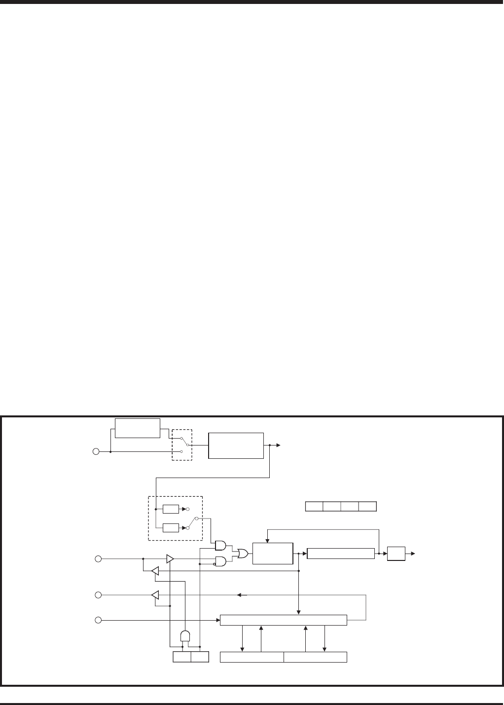
Figure 2.4.1 shows the serial I/O block diagram.
Fig. 2.4.1 Serial I/O block diagram
J1
2
SIOF
J1
2
J1
1
J1
0
J1
1
J1
0
MSB
1/4
1/8
1
0
P2
1
/S
OUT
P2
2
/S
IN
P2
0
/S
CK
TSIAB TABSI
S
OUT
S
IN
S
CK
J1
3
MR
3
1
0
X
IN
Division circuit
(divided by 2)
Internal clock
generation circuit
(divided by 3)
Instruction clock
Serial I/O mode register J1
Serial I/O interrupt
Serial I/O counter (3)
Synchronous
circuit
Register B (4)
Register A (4)
Serial I/O register SI (8)
LSB
Note: The output structure of S
CK
and S
OUT
pins is N-channel open-drain.


