4513/4514 Group User’s Manual
HARDWARE
1-13
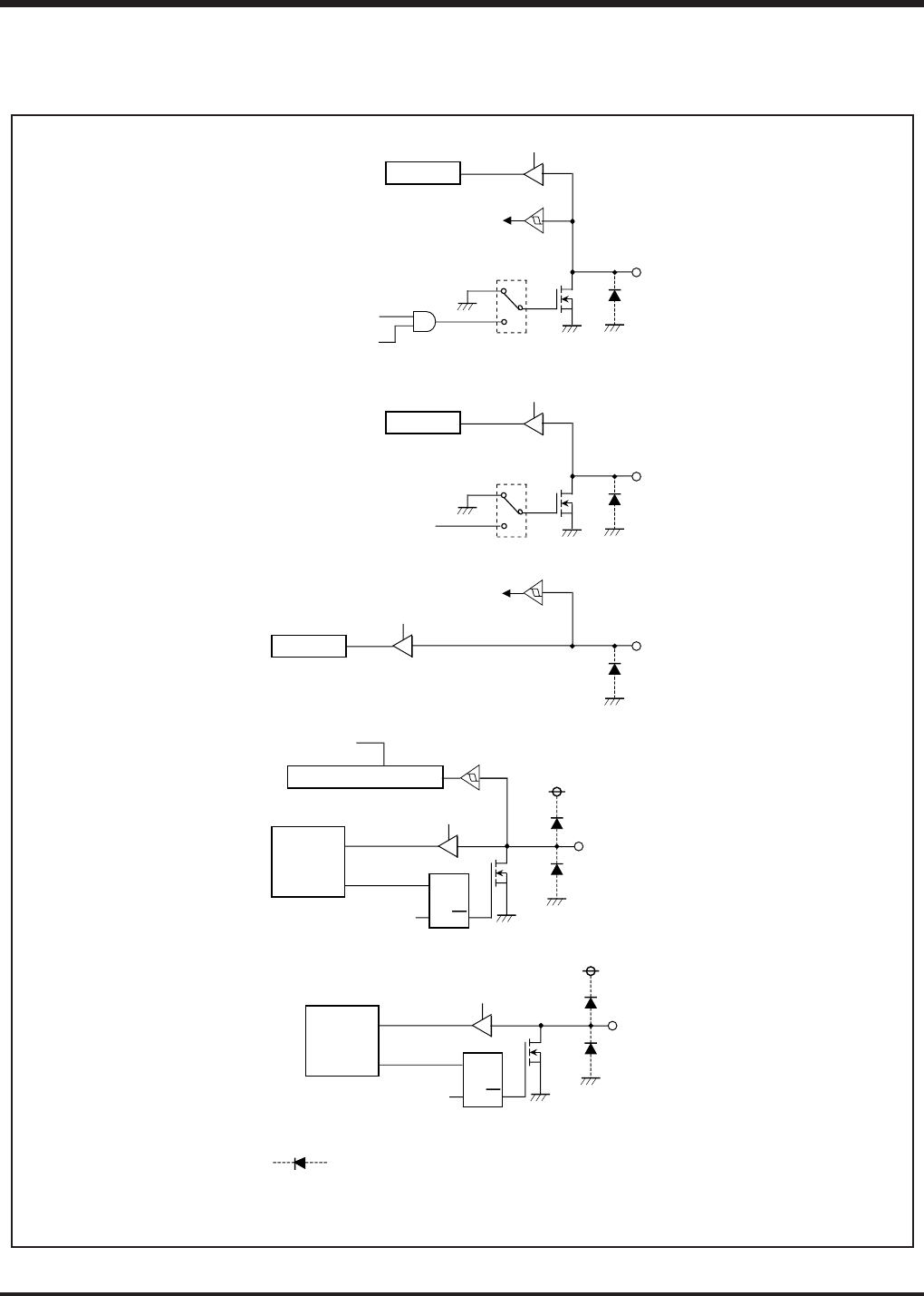
PORT BLOCK DIAGRAMS (continued)
PIN DESCRIPTION
Synchronous clock input for serial transfer
Register A
IAP2 instruction
P20/SCK
J1
0
Synchronous clock output for serial transfer
P30/INT0,P31/INT1
D
T
Q
External interrupt circuit
Register A
Ai
IAP3 instruction
OP3A instruction
J1
1
1
0
P21/SOUT
Register A
IAP2 instruction
Serial data output
J1
1
0
1
P22/SIN
Register A
IAP2 instruction
Serial data input
P32,P33
D
T
Register A
Ai
IAP3 instruction
OP3A instruction
Key-on wakeup input
This symbol represents a parasitic diode on the port.
• Applied potential to ports P2
0
—P2
2
must be V
DD
.
• i represents 0, 1, 2, or 3.
• The 4513 Group does not have ports P3
2
, P3
3
.
•
Q


