APPLICATION
2.5 A-D converter
2-52
4513/4514 Group User’s Manual
2.5.3 Notes on use
(1) Note when the A-D conversion starts again
When the A-D conversion starts again with the ADST instruction during A-D conversion, the previous
input data is invalidated and the A-D conversion starts again.
(2) A-D control register Q2
Select AIN4–AIN7 with register Q1 after setting register Q2.
(3) A-D converter-1
Each analog input pin is equipped with a capacitor which is used to compare the analog voltage.
Accordingly, when the analog voltage is input from the circuit with high-impedance and, charge/
discharge noise is generated and the sufficient A-D accuracy may not be obtained. Therefore, reduce
the impedance or, connect a capacitor (0.01 µF to 1 µF) to analog input pins.
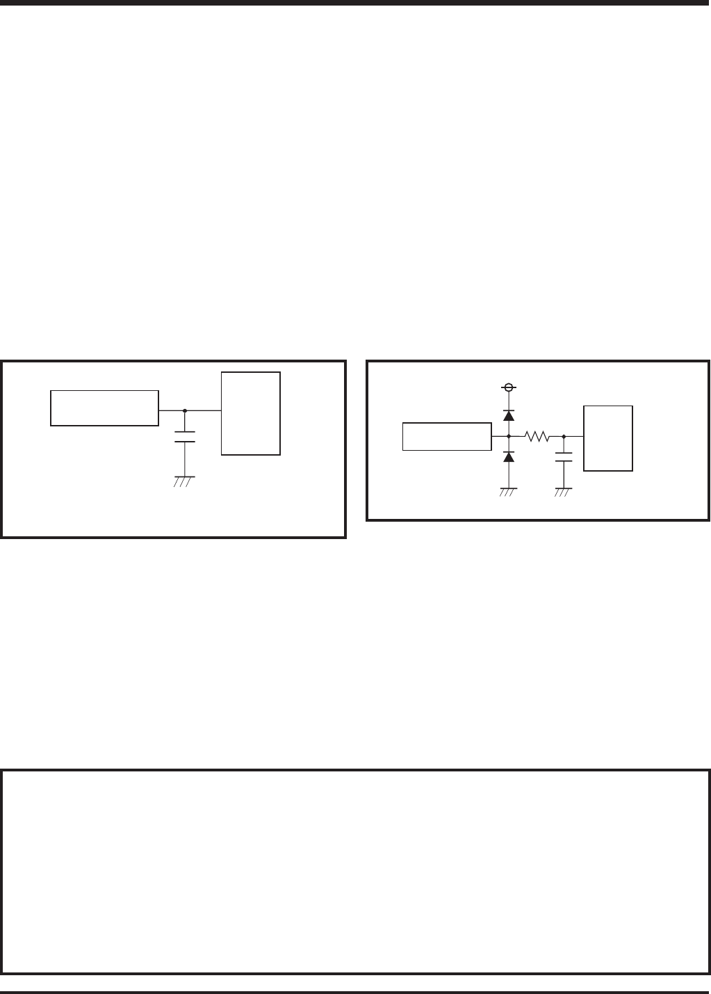
Figure 2.5.3 shows the analog input external circuit example-1.
When the overvoltage applied to the A-D conversion circuit may occur, connect an external circuit
in order to keep the voltage within the rated range as shown the Figure 2.5.4. In addition, test the
application products sufficiently.
Fig. 2.5.3 Analog input external circuit example-1
(4) Notes for the use of A-D conversion 2
When the operating mode of the A-D converter is changed from the comparator mode to the A-D
conversion mode with bit 3 of register Q2 in a program, be careful about the following notes.
• Clear bit 2 of register V2 to “0” to change the operating mode of the A-D converter from the
comparator mode to the A-D conversion mode with bit 3 of register Q2 (refer to Figure 2.5.5➀).
• The A-D conversion completion flag (ADF) may be set when the operating mode of the A-D
converter is changed from the comparator mode to the A-D conversion mode. Accordingly, set a
value to register Q2, and execute the SNZAD instruction to clear the ADF flag.
Do not change the operating mode (both A-D conversion mode and comparator mode) of A-D
converter with bit 3 of register Q2 during operating the A-D converter.
Fig. 2.5.4 Analog input external circuit example-2
Fig. 2.5.5 A-D converter operating mode program example
•
•
•
Clear bit 2 of register V2 to “0”.......➀
↓
Change of the operating mode of the A-D converter
from the comparator mode to the A-D conversion mode
↓
Clear the ADF flag to “0” with the SNZAD instruction
↓
Execute the NOP instruction for the case when a skip is
performed with the SNZAD instruction
•
•
•
Sensor AINi
(Note)
Note: i = 0 to 7
About 1 kΩ
Sensor
AINi
(Note)
Note: Apply the voltage within the specifications
to an analog input pin. (i = 0 to 7)
