APPLICATION
2-61
4513/4514 Group User’s Manual
2.9 RAM back-up
(2) Pull-up control register PU0
Pull-up control register PU0 controls the pull-up functions of ports P00–P03, P10–P13.
Set the contents of this register through register A with the TPU0A instruction. The TAPU0 instruction
can be used to transfer the contents of register PU0 to register A.
Table 2.9.5 shows the pull-up control register PU0.
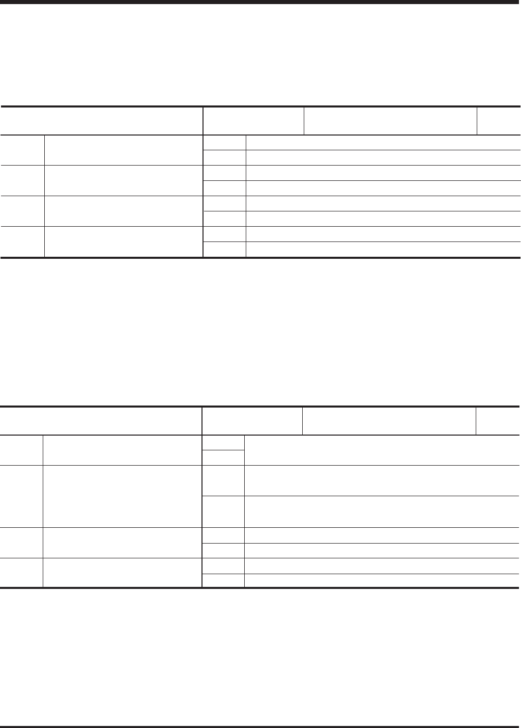
Table 2.9.5 Pull-up control register PU0
Pull-up control register PU0 at reset : 00002 at RAM back-up : state retained
R/W
Pull-up transistor OFF
Pull-up transistor ON
Pull-up transistor OFF
Pull-up transistor ON
Pull-up transistor OFF
Pull-up transistor ON
Pull-up transistor OFF
Pull-up transistor ON
Pins P12 and P13 pull-up
transistor control bit
Pins P10 and P11 pull-up
transistor control bit
Pins P02 and P03 pull-up
transistor control bit
Pins P00 and P01 pull-up
transistor control bit
0
1
0
1
0
1
0
1
PU03
PU02
PU01
PU00
Note: “R” represents read enabled, and “W” represents write enabled.
(3) Interrupt control register I1
The interrupt valid waveform for INT0 pin/return level selection bit is assigned to bit 2, INT0 pin edge
detection circuit control bit is assigned to bit 1, and INT0 pin timer 1 control enable bit is assigned
to bit 0.
Set the contents of this register through register A with the TI1A instruction.
In addition, the TAI1 instruction can be used to transfer the contents of register I1 to register A.
Table 2.9.6 shows the interrupt control register I1.
Table 2.9.6 Interrupt control register I1
Interrupt control register I1 at reset : 00002 at RAM back-up : state retained
R/W
This bit has no function, but read/write is enabled.
Falling waveform (“L” level of INT0 pin is recognized
with the SNZI0 instruction)/“L” level
Rising waveform (“H” level of INT0 pin is recognized
with the SNZI0 instruction)/“H” level
One-sided edge detected
Both edges detected
Disabled
Enabled
Not used
Interrupt valid waveform for INT0
pin/return level selection bit
(Note 2)
INT0 pin edge detection circuit
control bit
INT0 pin
timer 1 control enable bit
0
1
0
1
0
1
0
1
I13
I12
I11
I10
Notes 1: “R” represents read enabled, and “W” represents write enabled.
2: When the contents of I12 is changed, the external interrupt request flag EXF0 may be set.
Accordingly, clear EXF0 flag with the SNZ0 instruction.


