


M3062PT3-RPD-E User’s Manual 4. Hardware Specifications
REJ10J0040-0600 Rev.6.00 July 01, 2006 Page 77 of 104
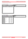
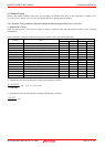
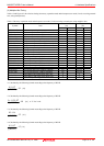
(3) Timing Requirements
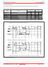
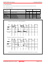
Table 4.4 and Figure 4.3 list the timing requirements in memory expansion mode and microprocessor mode.
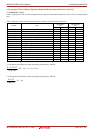
Table 4.4 Timing requirements
Actual MCU
[ns]
This product
[ns]
Symbol Item
Min. Max. Min. Max.
tsu(DB-RD)
Data input setup time 40 65
tsu(RDY-BCLK)
RDY# input setup time 30 55
tsu(HOLD-BCLK)
HOLD# input setup time 40 80
th(RD-DB)
Data input hold time 0 See left
th(BCLK-RDY)
RDY# input hold time 0 See left
th(BCLK-HOLD)
HOLD# input hold time 0 See left
td(BCLK-HLDA)
HLDA# output delay time 40 See left
* Compared with an actual MCU, this product enters high-impedance state after a 0.5 cycle delay.
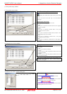
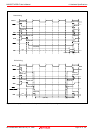
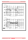
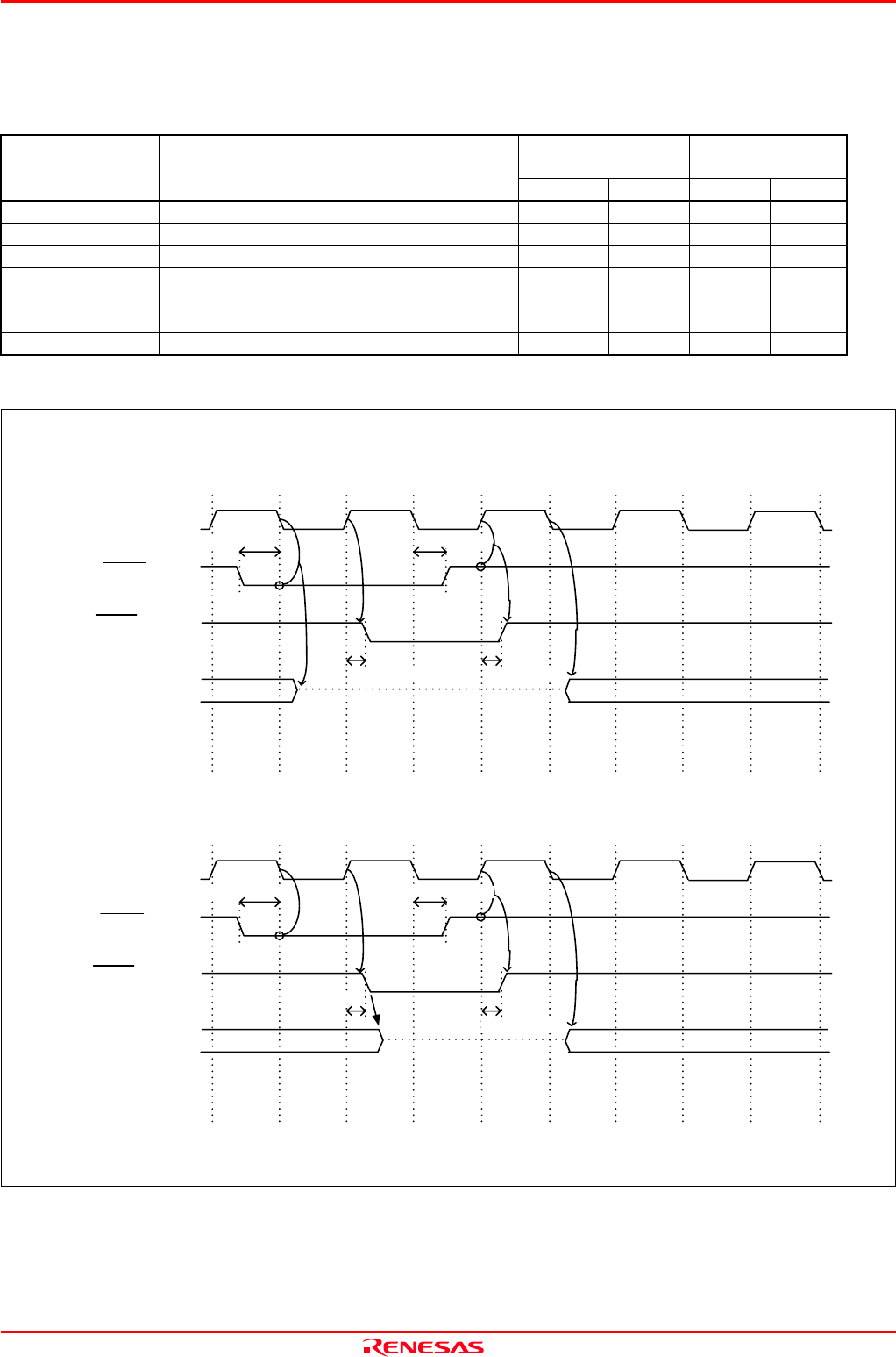
Figure 4.3 Timing requirements
Hi-Z
BCLK
P0,P1,P2,P3,P4,
P5
0 -- P52
tsu(HOLD-BCLK)
td(BCLK-HLDA)
td(BCLK-HLDA)
th(BCLK-HOLD)
Hi-Z
BCLK
P0,P1,P2,P3,P4,
P5
0 -- P52
tsu(HOLD-BCLK)
td(BCLK-HLDA)
th(BCLK-HOLD)
td(BCLK-HLDA)
HOLD input
HLDA output
HOLD input
HLDA output
Common to “with wait” and “no wait” (actual MCU)
Common to “with wait” and “no wait” (this product)