


M3062PT3-RPD-E User’s Manual 4. Hardware Specifications
REJ10J0040-0600 Rev.6.00 July 01, 2006 Page 86 of 104
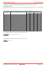
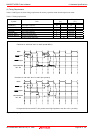
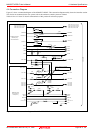
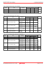
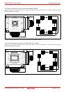
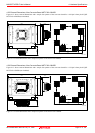
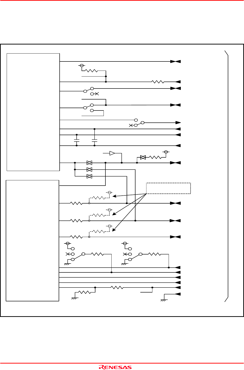
4.4 Connection Diagram
Figure 4.7 shows a connection diagram of the M3062PT3-RPD-E. This connection diagram mainly shows the interface section.
The circuits not connected to the user system such as the emulator's control system are omitted.
Tables 4.10 to 4.12 show IC electric characteristics of this product for reference purposes.
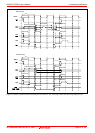
CNVss
BYTE
User system
33Ω
M30620T3-PRT
Port Emulation
FPGA(IC21)
P07--P00
RM2
Pull up resistors in dashed
line indicate that the socket is
mounted
Xin
33Ω
P27--P20
RM5
33Ω
P17--P10
P37--P30
P47--P40
P57--P50
P1:RM4
P3:RM6
P4:RM3
P5:RM1
P07--P00
P27--P20
Xin
CNVss
BYTE
M3062PT3-PRTM
M30627(IC2)
I/O Emulate MCU
P67--P60, P117--P110
P77--P70, P127--P120
P84--P80, P137--P130
P97--P90, P141,P140
P85/NMI#P85/NMI#
OPEN
SW4 P86/Xcout
P86/Xcout
P86/Xcout
SW5
P87
Xcin
P87/Xcin
P87/Xcin
XOUT
XOUT
SW3
OPEN
XOUT
C2 C3
AVCC
AVCC
VREF
VREF
AVSS
AVSS
*
100kΩ
Vcc1
*
*
Vcc2
Vcc2
Vcc2
51kΩ
51kΩ
51kΩ
P107--P100
Vcc1
51kΩ
*
AN7--AN0
SW1
33kΩ
SW2
1kΩ
1kΩ
Vcc1,Vcc2
Vcc1,Vcc2
510kΩ
Vss
Vcc1 Vcc1
*
P17--P10
P37--P30
P47--P40
P57--P50
74HC4066
P67--P60, P117--P110
P77--P70, P127--P120
P84--P80, P137--P130
P97--P90, P141,P140
7WH125
74HC4066
P107--P100
33Ω
RESET#
RESET#
100Ω
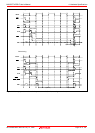
Figure 4.7 Part of the connection diagram of the M3062PT3-RPD-E