


M3062PT3-RPD-E User’s Manual 4. Hardware Specifications
REJ10J0040-0600 Rev.6.00 July 01, 2006 Page 94 of 104
IMPORTANT
Note on Stack Area:
z With this product, a maximum 7 bytes of the user stack is consumed. Therefore, ensure the +7 bytes
maximum capacity used by the user program as the user stack area. If the user stack does not have enough
area, do not use areas which cannot be used as stack (SFR area, RAM area which stores data, or ROM area)
as a work area. Using areas like this is a cause of user program crashes and destabilized emulator control.
Note on Operation When Not Executing the User Program:
z With this product, bit 7 of processor mode register 1 (wait bit PM17) is forcibly set to "1" (with wait) when
the user program is not executed (e.g. when the program is stopped or when run-time debugging is being
performed). Therefore, if the external area set to 0 wait is accessed by other than the user program (such as
debugging operation), one wait is inserted. However, when wait bit PM17 is referenced by the dump window
etc. the value set during user program execution is displayed.
Note on Stop and Wait Modes:
z Do not single step an instruction shifting to stop or wait mode. It may cause communication errors.
Note on Watchdog Function:
z The MCU's watchdog timer can be used only while programs are being executed. To use it otherwise, disable
the watchdog timer.
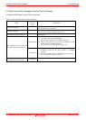
Note on Reading Internal Resources of the MCU:
z When the registers listed in Table 4.13 are read with an emulator, those results will be the following (the data
in the MCU are not effected).
(1) Results of real-time trace
The data values of the cycles read are not displayed correctly.
(2) Real-time RAM monitor
The data values read are not displayed correctly.
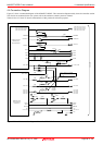
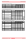
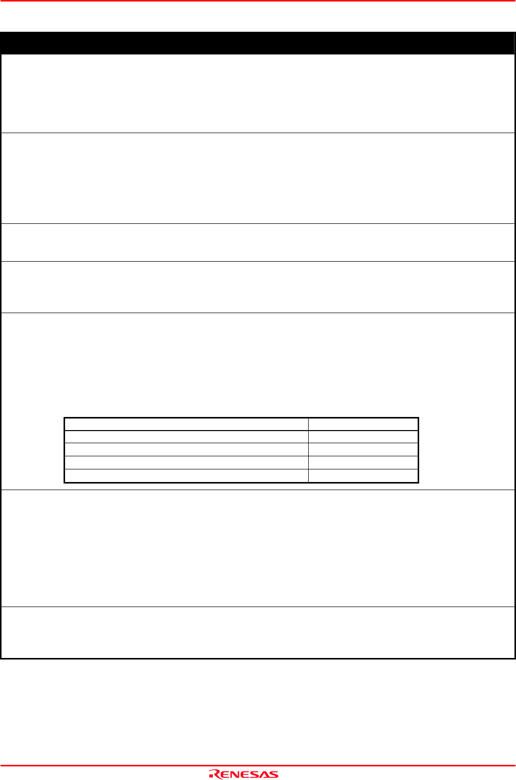
Table 4.13 Registers and symbols not displayed normally
Register
Symbol
DMA source pointers 0, 1 SAR0, SAR1
DMA destination pointers 0, 1 DAR0, DAR1
DMA transfer counters 0, 1 TCR0, TCR1
DMA control registers 0, 1 DM0CON, DM1CON
Note on Protect Register:
z The protect is not canceled when bit 2 of protect register PRCR (PRC2), which enables writing into the port
P9 direction register and the SI/Oi control register, is changed with the below procedure.
(1) Step execution of the "instruction for setting ("1") PRC2"
(2) Execution from the instruction setting "1" to PRC2 where a software breakpoint is set
(3) Setting the break point from the "instruction for setting ("1") PRC2" to when the "setting the port P9
direction register and the SI/Oi control register"
(4) Setting ("1") PRC2 from the Memory Window or Script Window
Note on Debugging in Flash Memory Area in CPU Rewrite Mode:
z With this product, an internal flash memory area of an MCU is emulated by high-speed SRAM. Therefore,
you cannot perform debugging operations in CPU rewrite mode.