


M3062PT3-RPD-E User’s Manual 4. Hardware Specifications
REJ10J0040-0600 Rev.6.00 July 01, 2006 Page 84 of 104
IMPORTANT
Note on RESET# Input:
z A low input from the user system to pin RESET# is accepted only while a user program is being executed
(only while the RUN status LED on the PC4701's front panel is lit).
Note on NMI# Input:
z A low input from the user system to pin NMI# is accepted only while a user program is being executed (only
while the RUN status LED on the PC4701's front panel is lit).
Note on RDY# Input:
z Be sure to input "L" to pin RDY# of the user system while a user program is being executed (when the RUN
status LED on the PC4701's front panel is lit). Inputting "L" to pin RDY# during the user program stopping
may cause a malfunction of the emulator.
Note on HOLD# Input:
z You cannot use the hold function with this product. Be sure to input "H" to pin HOLD# of the user system
when you use a processor mode other than single-chip mode. If "L" is input to pin HOLD#, this product will
not work normally.
Notes on Maskable Interrupts:
z Even if a user program is not being executed (including when run-time debugging is being performed), the
evaluation MCU keeps running so as to control the emulation pod. If a maskable interrupt is requested when
the user program is not being executed (including when run-time debugging is being performed), the
maskable interrupt request cannot be accepted, because the emulator disables interrupts. The interrupt request
is accepted immediately after the user program execution is started.
z Take note that when the user program is not being executed (including when run-time debugging is being
performed), a peripheral I/O interruption is not accepted.
Note on DMA Transfer:
z With this product, the program is stopped with a loop program to a specific address. Therefore, if a DMA
request is generated while the program is stopped, a DMA transfer is executed, but it may not be performed
correctly. Also note that the below registers have been changed to generate a DMA transfer as explained here
even when the program is stopped.
DMA0 transfer counter registers : TCR0
DMA1 transfer counter registers : TCR1
Note on Pullup Control:
z With this product, ports P0 to P5 are not pulled up by the pullup control register. To pull up the ports P0 to
P5, mount the included network resistor (51kΩ) to the inside of the emulator as occasion demands. How to
mount it, refer to "2.9.6 Installing and Removing Network Resistors for Pullup" (page 48).
z The initial value of pullup control register 1 (PUR1) of an actual MCU varies depending on the level of the
CNVss pin, while that of this product is always “00h”.
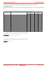
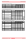
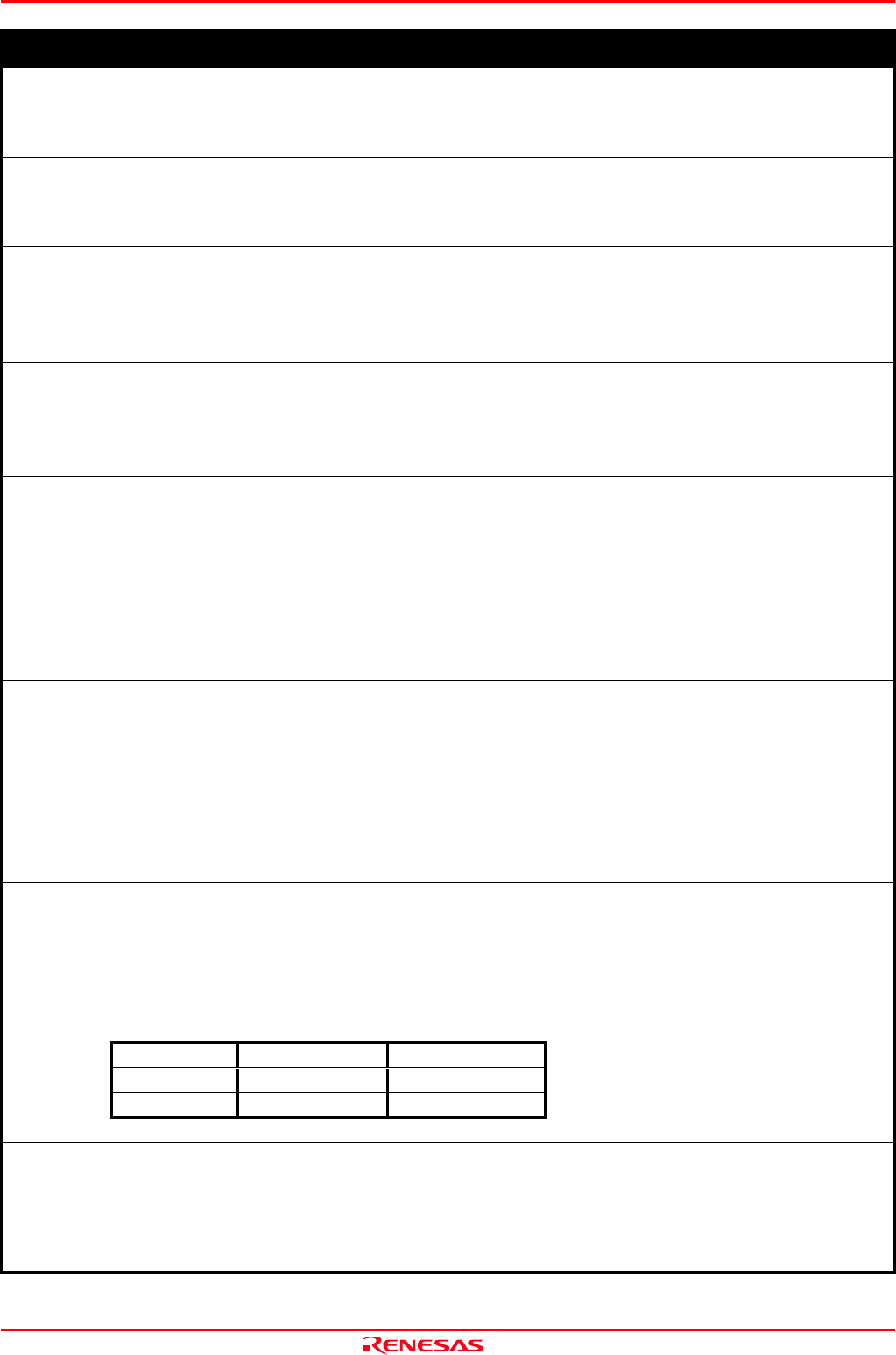
Table 4.9 Initial value of pullup control register 1 (PUR1)
CNVss = “L” CNVss = “H”
Actual MCU PUR1 = “00h” PUR1 = “02h”
This product PUR1 = “00h” PUR1 = “00h”
Note on Setting "1" to Protect Bit 2 (PCR2) with Sub Clock:
z When the CPU clock is set to the sub-clock (low-speed mode or low power dissipation mode), even if you
enable the PRC2 bit, writing to the register protected by the PRC2 bit (PD9, S3C, and S4C registers) cannot
be done properly. When you enable the PRC2 bit and write to the register protected by the PRC2, do not set
the CPU clock to the sub-clock.