Signal Connections for In-System Programming and Debugging
www.ti.com
2.1 Signal Connections for In-System Programming and Debugging
MSP-FET430PIF, MSP-FET430UIF, MSP-GANG430, MSP-PRGS430
With the proper connections, the debugger and an FET hardware JTAG interface (such as the
MSP-FET430PIF and MSP-FET430UIF) can be used to program and debug code on the target board. In
addition, the connections also support the MSP-GANG430 or MSP-PRGS430 production programmers,
thus providing an easy way to program prototype boards, if desired.
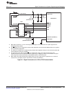
Figure 2-1 shows the connections between the 14-pin FET interface module connector and the target
device required to support in-system programming and debugging for 4-wire JTAG communication.
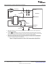
Figure 2-2 shows the connections for 2-wire JTAG mode (Spy-Bi-Wire). While 4-wire JTAG mode is
supported on all MSP430 devices, 2-wire JTAG mode is available on selected devices only. See the CCS
User's Guide for MSP430 (SLAU157) or IAR for MSP430 User's Guide (SLAU138) for information on
which interface method can be used on which device.
The connections for the FET interface module and the MSP-GANG430 or MSP-PRGS430 are identical.
Both the FET interface module and MSP-GANG430 can supply V
CC
to the target board (via pin 2). In
addition, the FET interface module and MSP-GANG430 have a V
CC
-sense feature that, if used, requires
an alternate connection (pin 4 instead of pin 2). The V
CC
-sense feature senses the local V
CC
present on the
target board (i.e., a battery or other local power supply) and adjusts the output signals accordingly. If the
target board is to be powered by a local V
CC
, then the connection to pin 4 on the JTAG should be made,
and not the connection to pin 2. This utilizes the V
CC
-sense feature and prevents any contention that might
occur if the local on-board V
CC
were connected to the V
CC
supplied from the FET interface module or the
MSP-GANG430. If the V
CC
-sense feature is not necessary (i.e., the target board is to be powered from the
FET interface module or the GANG430) the V
CC
connection is made to pin 2 on the JTAG header and no
connection is made to pin 4. Figure 2-1 and Figure 2-2 show a jumper block that supports both scenarios
of supplying V
CC
to the target board. If this flexibility is not required, the desired V
CC
connections may be
hard-wired eliminating the jumper block. Pins 2 and 4 must not be connected simultaneously.
Note that in 4-wire JTAG communication mode (see Figure 2-1), the connection of the target RST signal
to the JTAG connector is optional when using devices that support only 4-wire JTAG communication
mode. However, when using devices that support 2-wire JTAG communication mode in 4-wire JTAG
mode, the RST connection must be made. The MSP430 development tools and device programmers
perform a target reset by issuing a JTAG command to gain control over the device. However, if this is
unsuccessful, the RST signal of the JTAG connector may be used by the development tool or device
programmer as an additional way to assert a device reset.
24
Design Considerations for In-Circuit Programming SLAU278F–May 2009–Revised December 2010
Submit Documentation Feedback
© 2009–2010, Texas Instruments Incorporated


