Major Chips Description 2-43
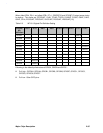
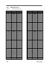
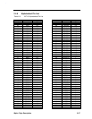
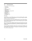
2.5.4 Pin Descriptions
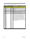
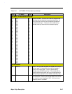
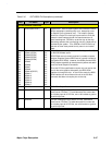
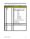
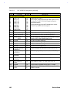
Table 2-10 C&T 65550 Pin Descriptions
Pin# Pin Name Type Description
CPU Direct / VL-Bus Interface
207 RESET In Reset. For VL-Bus interfaces, connect to RESET#. For
direct CPU local bus interfaces, connect to the system reset
generated by the mother board system logic for all
peripherals (not the RESET# pin of the processor). This
input is ignored during Standby mode (STNDIBY# pin low) so
that the remainder of the system (and the system bus) may
be safely powered down during Standby mode if desired.
22 ADS# In Address Strobe. In VL-Bus and CPU local bus interfaces
ADS# indicates valid address and control signal information
is present. It is used for all decodes and to indicate the start
of a bus cycle.
31 M/IO# In Memory /IO. In VL-Bus and CPU local bus interfaces M/lO#
indicates either a memory or an I/O cycle:
1 = memory, 0 = I/O
11 W/R# In Write / Read. This control signal indicates a write (high) or
read (low) operation. It is sampled on the rising edge of the
(internal) 1x CPU clock when ADS# is active.
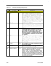
23 RDYRTN# for 1x Clock
config
CRESET for 2x Clock
config
In Ready Return. Handshaking signal in VL-Bus interface
indicating synchronization of RDY# by the local bus master /
controller to the processor. Upon receipt of this LCLK-
synchronous signal the chip will stop driving the bus (if a read
cycle was active) and terminate the current cycle.
24 LRDY# Out/
OC
Local Ready. Driven low during VL-Bus and CPU local bus
cycles to indicate the current cycle should be completed This
signal is driven high at the end of the cycle, then tri-stated.
This pin is tri-stated during Standby mode (as are all other
bus interface outputs).
25 LDEV# Out Local Device. In VL Bus and CPU local bus interfaces. this
pin indicates that the chip owns the current cycle based on
the memory or l/O address which has been broadcast. For
VL-Bus, it is a direct output reflecting a straight address
decode. This pin is tri-stated during Standby mode (as are all
other bus interface outputs).
27 LCLK In Local Clock. In VL Bus this pin is connected to the CPU 1x
clock. In CPU local bus interfaces it is connected to the CPU
1x or 2x clock. If the input is a 2x clock, the processor reset
signal must be connected to CRESET (pin 23) for
synchronization of the clock phase.


