Major Chips Description 2-11
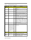
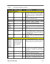
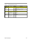
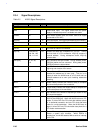
Table 2-2 M1521 Signal Descriptions (continued)
Signal Pin Type Description
Secondary Cache Interface
CCSJ/CB4 W16 O Synchronous SRAM chip select or Cache Address
line 4 copy. This pin has two modes of operation
depending on the type of SRAM selected via
hardware strapping options or programming the CC
register.
GWEJ Y16 O Synchronous SRAM Global Write Enable or
Asynchronous SRAM Write Enable.
COEJ U15 O Synchronous/Asynchronous SRAM Output Enable.
BWEJ/CGCSJ Y17 O Synchronous SRAM Byte-Write Enable/
Asynchronous SRAM Global Chip Select.
TIO[10]/
MWEJ[1]
Y20 I/O SRAM Tag[10] or another copy of MWEJ.
TIO[9]/
SRASJ[1]
Y19 I/O SRAM Tag[9] or synchronous DRAM (SDRAM) RAS
copy 1.
TIO[8]/
SCASJ[1]
W19 I/O SRAM Tag[8] or synchronous DRAM (SDRAM) CAS
copy 1.
TIO[7:0] Y18, W18, V18, T14,
V17, U17, U16, P16
I/O SRAM Tag[7:0]. This pin contains the L2 tag
address for 256 KB L2 caches. TIO[6:0] contain the
L2 tag address and TIO7 contains the L2 cache valid
bit for 512 KB caches.
TWEJ V16 O Tag Write Enable. This signal, when asserted,
writes into the external tag new state and tag
addresses.
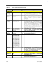
PCI Interface
AD[31:28]
AD[27:24]
AD[23:20]
AD[19:16]
AD[15:12]
AD[11:08]
AD[07:04]
AD[03:00]
A2, B2, A3, B3, A4, B4,
C4, D6, B5, C5, A6, B6,
C6, A7, B7, C7, C8, A9,
B9, C9, A10, B10, C10,
A11, C11, A12, B12,
C12, A13, B13, A14,
A15
I/O PCI Address-and-Data Bus Lines. These lines
connect to the PCI bus. AD[31:0] contain the
information of address or data for PCI transactions.
CBEJ[3:0] A5, A8, B8, B11 I/O PCI Bus Command and Byte Enables. Bus
commands and byte enables are multiplexed in
these lines for address and data phases,
respectively.
FRAMEJ E6 I/O Cycle Frame of PCI Buses. This indicates the
beginning and duration of a PCI access.
DEVSELJ E9 I/O Device Select. When the target device has decoded
the address as its own cycle, it asserts DEVSELJ.
IRDYJ E7 I/O Initiator Ready. This indicates the initiator is ready
to complete the current data phase of transaction.


