Major Chips Description 2-9
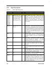
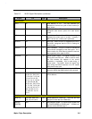
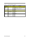
Table 2-2 M1521 Signal Descriptions (continued)
Signal Pin Type Description
Host Interface
M/IOJ H5 I Host Memory or I/O. This bus definition pin
indicates the current bus cycle is either memory or
input/ output.
D/CJ T7 I Host Data or Code. This bus definition pin is used to
distinguish data access cycles from code access
cycles.
W/RJ T9 I Host Write or Read. When WRJ is driven high, it
indicates the current cycle is a write. Inversely, if
WRJ is driven low, a read cycle is performed.
HLOCKJ G5 I Host Lock. When HLOCKJ is asserted by the CPU,
the M1521 recognizes that the CPU is locking the
current cycles.
CACHEJ J5 I Host Cacheable. This pin is used to indicate the
host’s internal cacheability of the read cycles. If it is
driven inactive, the CPU does not cache the returned
data regardless of the state of KENJ.
KENJ/INV K5 O Cache Enable Output. This signal connects to the
CPU's KENJ and INV pins. KENJ is used to notify
the CPU whether the address of the current
transaction is cacheable. INV is used during L1
snoop cycles. The M1521 drives this signal high
(low) during the EADSJ assertion of a PCI master
write (read) snoop cycle.
SMIACTJ T10 I SMM Interrupt Active. It is asserted by the CPU to
inform the M1521 that SMM mode is being entered.
HD[63:0] A1, B1, C3, C2, C1, D2,
D3, E3, D1, E2, E4, E1,
F3, F4, G3, F1, F2, H3,
G1, H4, G4, J3, G2,
H2, H1, J4, J1, J2, M4,
K1, M2, M3, N4, N2,
N3, P4, N1, P2, P3, R4,
P1, T2, R2, T4, R3, U2,
T3, U4, V2, U3, V4, T1,
W4, V3, W3, U1, R1,
V1, W2, W1, Y4, Y2,
Y3, Y1
I/O Host Data Bus Lines. These signals connect to the
CPU's data bus.
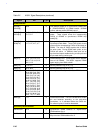
DRAM Interface
MPD[7:0] G18, H20, G20, H18,
F20, J18, G19, H19
I/O DRAM Parity/ECC check bits. These are the 8-bit
parity/ECC check bits over DRAM bus.
RASJ[7] /
SRASJ[0]
N16 O Row Address Strobe 7 or Synchronous DRAM RAS
0. FPM/EDO/BEDO of DRAM bank 7. SDRAM row
address strobe (SDRAM) copy 0.


