2-10 Service Guide
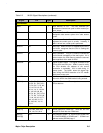
Table 2-2 M1521 Signal Descriptions (continued)
Signal Pin Type Description
DRAM Interface
RASJ[6] /
SCASJ[0]
M16 O Row Address Strobe 6, or Synchronous DRAM CAS
0 (FPM/EDO/BEDO) of DRAM bank 6. SDRAM
column address strobe (SDRAM) copy 0.
RASJ[5:0] /
SCSJ[5:0]
N17, M17, E16, F16,
F17, G17
I/O Row Address Strobes or synchronous DRAM chip
select. These signals drives the corresponding
RASJs of DRAMs or synchronous DRAM chip
select[5:0].
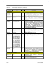
CASJ[7:0] /
DQM[7:0]
L16, G16, J16, H16,
L17, H17, K17, J17
O Column Address Strobes or Synchronous DRAM
Input/Output Data Mask. These CAS signals should
connect to the corresponding CASJs of each bank of
DRAM. The value of CASJs equals that of HBEJs
for write cycles. During DRAM read cycles, all the
CASJs are active. In SDRAM, these pins act as
synchronized output enables during a read cycle and
a byte mask during a write cycle.
MA[11:2] V14, Y14, Y15, U14,
W14, T13, U13, V13,
W13, Y13
O DRAM Address lines. These signals are the address
lines of all DRAMs. The M1521 supports DRAM
types ranging from 256K to 64M.
MAA[1:0] T12, V12 O Memory Address copy A for [1:0]
MAB[1:0] U12, W12 O Memory Address copy B for [1:0]
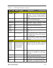
MD[63:0]
C15, A16, B17, A18,
B19, B20, D19, E20,
J19, K20, M18, N19,
P20, R19, T18, V20,
C14, D15, C16, D17,
A20, C20, E18, F19,
K18, L19, M20, P18,
R17, T20, U19, V19,
B14, D16, A17, C17,
A19, D18, E17, E19,
J20, L18, M19, N20,
P17, R18, U20, U18,
C13, B15, B16, B18,
C18, C19, C20, F18,
K19, L20, N18, P19,
R20, T19, T17, W20
I/O Memory Data. These pins connect to DRAMs.
MWEJ[0] T11 O DRAM Write Enable. This is the DRAM write enable
pin and behaves according to the early-write
mechanism; i.e. it activates before the CASJs do.
For refresh cycles, it remains deasserted.
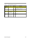
Secondary Cache Interface
CADVJ/CA4 V15 O Synchronous SRAM advance or Asynchronous
SRAM address line 4.
CADSJ/CA3 W15 O Synchronous SRAM address strobe cache or
Asynchronous SRAM address line 3.


