2-48 Service Guide
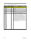
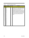
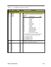
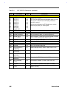
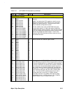
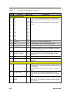
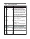
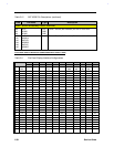
Table 2-10 C&T 65550 Pin Descriptions (continued)
Pin# Pin Name Type Description
PCI Bus Interface (continued)
51
50
49
48
47
46
45
44
41
40
38
37
36
35
34
33
20
19
18
17
16
15
14
13
8
7
6
5
4
3
2
1
AD00
AD01
AD02
AD03
AD04
AD05
AD06
AD07
AD08
AD09
AD10
AD11
AD12
AD13
AD14
AD15
AD16
AD17
AD18
AD19
AD20
AD21
AD22
AD23
AD24
AD25
AD26
AD27
AD28
AD29
AD30
AD31
I/O
I/O
I/O
I/O
I/O
I/O
I/O
I/O
I/O
I/O
I/O
I/O
I/O
I/O
I/O
I/O
I/O
I/O
I/O
I/O
I/O
I/O
I/O
I/O
I/O
I/O
I/O
I/O
I/O
I/O
I/O
I/O
PCI Address / Data Bus. Address and data are multiplexed
on the same pins. A bus transaction consists of an address
phase followed by one or more data phases (both read and
write bursts are allowed by the bus definition).
The address phase is the clock cycle in which FRAME# is
asserted (AD0-31 contain a 32-bit physical address). For I/O,
the address is a byte address; for memory and configuration,
the address is a DWORD address. During data phases AD0-
7 contain the LSB and 24-31 contain the MSB. Write data is
stable and valid when IRDY# is asserted; read data is stable
and valid when TRDY# is asserted. Data transfers only
during those clocks when both IRDY# and TRDY# are
asserted.


