


10
Because strobe edges are centered on the data valid window for writes, and straddle it
for reads, the analyzer cannot simply use the raw DQS0 to sample data. If it did, then
even in the ideal case, only half of the data valid window would be usable. In practice, it
would almost completely disappear. To deal with this, the DDR Probe adjusts the timing
of DQS0 before sending it to the analyzer state clock input by delaying it a fixed amount
for reads. This is done using a socketed delay line, which is set at the factory and
should be sufficient. If EyeFinder results show good eyes when the probe is set to pass
Reads only and Writes only (SW #6 off), but the eyes are significantly reduced when the
probe passes BOTH Reads and Writes (SW #6 on), then the delay value on the probe
may need adjustment. The calibration procedure documented in this User Manual
describes how to set the probe delay line and analyzer sample position for reliable state
analysis operation.
Because the strobes are tristated between bursts their logic value is undefined. Some
systems will terminate the DDR bus to a voltage close to the Vref voltage, causing the
strobes to sit right at the switching threshold. During read bursts, because read data
(and strobes) are actually not valid until the reflected wave reaches the probe, DQS0
may also spend a significant amount of time at Voh/2 (close to Vref) between arrival of
the incident wave and the reflected wave. Therefore, simply comparing the DQS0 signal
to Vref will result in spurious analysis clocks being generated between bursts and during
read bursts. The DDR probe deals with these factors by recognizing valid DQS0 edges
only when they are closer to Vih than Vref as well as by inhibiting the state clock
between bursts. In actual operation enough noise immunity is added by the special
DQS0 receiver circuit to eliminate almost all spurious data strobes without inhibiting the
clock.
All of these factors combine to add jitter to the read and write strobes sensed by the
DDR probe. This jitter reduces the data valid window available to the logic analyzer. In
some systems and DIMM configurations that have tight bus timing this may make it
difficult to find an appropriate point to sample state data. This is especially true for read
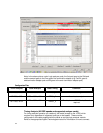
bursts that usually have more complex strobe and data waveforms. Eye Finder will
measure the data valid window available to the analyzer for each signal and clearly
indicate which ones may have difficulty reliably sampling state data given actual DDR
bus timing.