


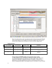
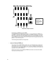
21
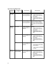
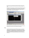
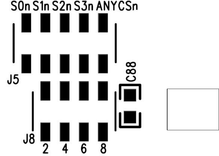
Chip Select Jumper locations
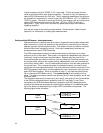
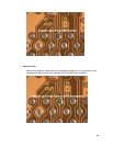
2) Dedicating a DIMM slot to the FS2331
This approach offers the highest signal integrity. It involves dedicating a DIMM slot to
the FS2331, isolating the Chip Select signals on that DIMM connector from the target’s
DDR bus and then wiring active Chip Select signals from all active DIMMs over to the
probe’s DIMM connector. Please note that this requires that the appropriate jumpers be
placed on J5 per the table above.
The following photos detail this wiring process.
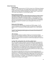
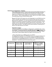
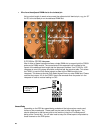
§ Isolate the Dedicated DIMM’s pin.
The standard 184 pin DDR DIMM connector has the 4 Chip Select lines routed to the
following pins: pin 157 (S0), pin 158 (S1), pin 71 (S2), pin 163 (S3). Most applications
will require just S0 single sided DIMMs) or S1 (double-sided DIMMs) to be isolated and
jumpered from the active DIMM slot.
Identify the correct pin on the dedicated DIMM slot connector and remove the solder
from the pin and hole as shown.
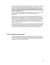
Factory config is
J8 pin 1&2
jumpered. This
must be removed
if J5 connections
are used.