


27
3. Trigger the analyzer on any burst.
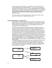
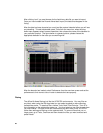
4. Open a new All Waves waveform window that displays measurement results from
both the Command and Data analyzers. This can be done from the Workspace
window by dragging a waveform display tool onto the Workspace and connecting
the output of each Data and Command analyzer to the tool.
5. Insert the labels DATA_TZ:BUFFCMDCLK_TZ and
COMMAND_TZ:BUFFCMDCLK_TZ onto the waveform window.
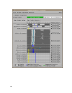
6. Find corresponding edges of both labels and note the time difference between them
as displayed in the waveform window. You may need to set the display scale to
less than 5ns/division to do this properly. You can do this very accurately by placing
the G1 marker on one edge and the G2 marker on the corresponding edge of the
other label. The time difference between the markers will be displayed in a small
popup window for about 5 seconds.
7. Open the "Intermodule Skew..." dialog of the "Window->System->Intermodule..."
window and modify the entry corresponding to the Data analyzer as follows:
If DATA_TZ:BUFFCMDCLK_TZ edges are after (before)
COMMAND_TZ:BUFFCMDCLK_TZ then add (subtract) the time difference
displayed in the waveform to the current skew value and enter the new value.
8. Press the "Apply" button. The waveform display will be updated and should show
the DATA_TZ:BUFFCMDCLK_TZ and COMMAND_TZ:BUFFCMDCLK_TZ signals
occurring within 1ns of each other. You may go back to step 8 if you wish, repeating
as necessary to find the correct Intermodule skew adjustment value.
If you save the analyzer configuration for all modules then the skew adjustment will be
saved as well. This calibration may need to be repeated from time to time to ensure that
the skew remains minimized.
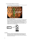
The Inverse Assembler and Decoding DDR Commands
The inverse assembler has an optional feature that will match a read or write command
with its corresponding ACTIVATE command for the same bank and DIMM, and display a
complete row/column address for the read or write command. The ADDR_B label is
used for this purpose, and has been defined on the same logic analyzer channels as the
Chip Select and Bank Address labels so that it can know which DIMM is being issued a
given READ, WRITE, or ACTIVATE command. This feature may be turned on and off in
the dialog that is displayed by selecting the “Invasm/Preferences” menu pick. When it is
turned off the inverse assembler will display only the column and bank address passed
to the READ or WRITE Command (as well as the Command itself).
Symbols are pre-defined for the DDR Command bus. These decode the RAS, CAS,
and WE lines to display the DDR command as “Read”, “Write”, “Precharge”, etc., so you
don’t have to refer to the DDR chip data sheet to see what command is being executed.
Symbols have also been pre-defined for the read/write status generated by the probe.
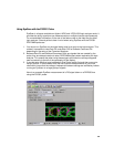
Taking a Trace, Triggering, and Seeing Measurement Results
For state analysis measurements both the DDR Command and Data busses are
captured, each by a separate logic analyzer module. The 167xx and 169xx Intermodule
Bus is used to communicate triggering information between the modules. The default
analyzer configurations shipped with the FS2331 for state measurements pre-configures
a trigger in which a specified Command is detected and causes a trigger of the