


39
•
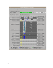
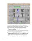
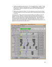
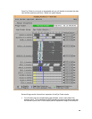
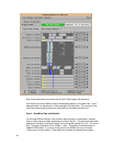
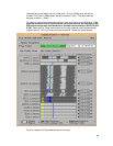
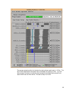
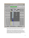
Not all channels have a data valid window after the clock. This is because the clock
for data bursts is active on both rising and falling edges of the strobe. When the
Eye Finder measurement looks at the time period after the strobe, it sometimes is
looking at the data line after the end of a burst (which will occur after the last falling
edge of the strobe). The data will not always be stable at that time, so Eye Finder
will sometimes see no data valid window after the strobe.
•
The data valid windows appear to be about 1.5ns in size for the Data signals.
Actual measurement with a scope showed the windows were actually closer to
2.5ns. Eye Finder is really measuring how much larger the data valid window is
than the actual window required by the analyzer at the time of the measurement.
Eye sizes measured with a scope will typically be about 1ns larger than those
indicated on the Eye Finder display. Even if a window shows up as only a few
hundred picoseconds in width in the Eye Finder display, you should be able to
capture state data since the actual data valid window will be 1.25ns or more. This
reemphasizes that the Eye Finder results should not be treated as definitive,
quantitative data. They can however help you rapidly sort through dozens of signals
to find the few that deserve closer examination.
•
Eye Finder did not always choose to suggest a sample position that is on the same
side of the clock for all channels. In general, Eye Finder will choose the data valid
window that is closest to time 0 (the clock).
•
The DataClk is not stable around time 0. This is to be expected since time 0 is the
point where DataClk rises or falls. The data valid windows around time 0 are about
the same size, indicating a 50% duty cycle for the strobe.
•
The unstable regions of DataClk around +- 3 / 4 ns are fairly large. This may
indicate actual clock jitter or jitter added by the probe when receiving DQS0. More
detailed examination with a scope can help identify the sources of the jitter.
•
The positions of the data valid windows for the data lines are close but not identical.
This is due to measurement uncertainty as well as actual skews due to DRAM,
DIMM, DDR probe and motherboard layout. It can also be an artifact of the stimulus
if effects such as inter-symbol interference or simultaneous switching effects are not
uniformly distributed across all data lines. If there is too much skew, that would be
an indication that closer examination with a scope may be warranted.
•
The strobe lines are offset from the data lines by one quarter cycle. This is correct
behavior for write cycles. Note that the strobes precede the analyzer clock due to
the propagation delay of the DQS0 processing circuitry that generates the analyzer
clock. While the edges of the strobes are properly centered on the data valid
windows for these write bursts, the analyzer clock is not centered. This is normal
and acceptable since the analyzer sample position will be adjusted in step 5 to
sample data at the proper time relative to DQS0.
•
The ECC bits of the DIMM were being used as indicated by the activity on the CB
lines.
•
The Serial Presence Detect lines are stable. This is normal when making
measurements after the DDR bus controller has completed its initialization of the
bus.