


20
Connecting to your Target System – Chip Select
Many DDR333 systems qualify Command activity using the Chip Select lines, S0:3. This
is either because they utilize “2T Timing” in which their control lines (RAS, CAS, WE)
may not fully transition to a valid state within one command clock, or because NOP
commands are indicated only by releasing all chip selects rather than issuing an actual
NOP command. Either of these conditions will make it difficult for the FS2331 to decode
Commands properly without valid Chip Select signals.
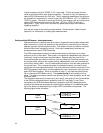
Because Chip Select (S0:3) signals are routed independently to each DIMM slot and the
FS2331 consumes a slot, the probe will not normally be able to see which memory a
given command is directed to. As a result the probe cannot properly decode activity on
DIMMs that is qualified by these signals unless they are brought to the probe. On some
systems this will be seen as small or missing Data eyes after running Eyefinder . This
problem can be corrected if the chip select signals for all memory ranks to be traced are
made visible to the probe. The FS2331 user has several means for connecting up to 4
different Chip Select signals to the FS2331.
Chip Select Jumpers
The factory configuration of the FS2331 is a single jumper on J8 between pins 1 and 2.
This forces S0 low (active) on the FS2331 and effectively qualifies ANY Command seen
by the FS2331. This may be sufficient for the proper operation in your target system. If it
is not, then there are 3 ways to bring active Chip Select signals to the FS2331. Please
note that each of these methods requires all jumpers to be removed from J8.
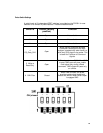
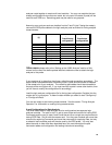
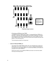
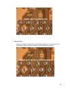
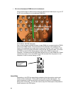
1) Wiring Chip Select from a DIMM module to the FS2331
Four test points are provided on the DDR probe to allow you to probe Chip Selects from
other DIMM slots on the target. You must solder a wire from the DIMM module and
connect the wire to the appropriate test point on the FS2331. A table showing jumper
configurations is provided. GND points are on J8 pins 2, 4, 6, and 8 to allow the use of
twisted pairs . You should keep the wires as short as possible.
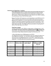
Chip Select line
Remove jumper
(factory config)
Connect wire from
another DIMM to
If User is dedicating a
DIMM slot, or using an
Interposer (FS1024 or
1025) add
S0 J8 pins 1 and 2 J5 pin 2 Jumper J5 pins 1 and 2
S1 J5 pin 4 Jumper J5 pins 3 and 4
S2 J5 pin 6 Jumper J5 pins 5 and 6
S3 J5 pin 8 Jumper J5 pins 7 and 8
AnyCS (special) J5 pin 10 Jumper J5 pins 9 and 10