


9
Probe Design
This probe uses discrete ECL logic in order to operate at the speed necessary to
provide DDR333 signal decode. Because ECL logic operates in linear mode it dissipates
more heat than other logic designs.
BE ADVISED – THE PROBE IS HOT TO THE TOUCH. . If the user believes that the
FS2331’s temperature is above 80°C, then a fan should be used to provide
additional cooling.
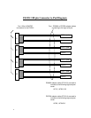
In order to support source synchronous data capture the FS2331 DDR probe monitors
the clock (CK0/CK0n) and control (DQS0, CAS, RAS, WE, S0:3) signals on the DIMM
connector where the probe is inserted. In some cases the probe may also need access
to the chip select signals for other DIMM slots to enable source synchronous data
capture. There may be situations where these signals are not provided by the target
system. For instance, some systems may turn off CK0 to slots where no DIMM module
is detected. In other systems, the unique Chip Select signals for each DIMM may need
to be connected to the probe.
If there is any reason to suspect that these conditions are present on your target,
contact FuturePlus Technical Support.
State Clock Generation
The FS2331 DDR probe uses one logic analyzer machine to capture DDR commands
(using the common clock CK0) and another machine to capture DDR burst data (using
the source synchronous strobe DQS0). The logic analyzer automatically combines the
trace data from both machines into a single time correlated trace of DDR bus activity.
The circuitry on the probe is used to generate the proper state analysis clocks for the
command and data analysis machines.
DDR Commands
Since the DDR bus global clock is differential it is converted to a single ended clock for
the analyzer using a differential line receiver. DDR Commands are sampled on the
rising edge of this clock.
DDR Data
The FS2331 supports state analysis of DDR busses by combining a specially processed
version of the DQS0 strobe with Agilent's Eye Finder technology. This allows the
analyzer/probe combination to accurately locate (much as a DDR controller chipset
does) the read and write data valid windows for each data bus signal and sample the
data at the proper time for reliable state analysis.
Each DDR bus implementation will have different timing due to trace length variation on
the motherboard, variations in bus loading for each DIMM configuration, and sensitivity
to dynamic factors such as crosstalk or simultaneous switching noise. Therefore, the
precise position of the DDR data eye will vary from system to system and even within a
system as DIMM configurations or data access patterns change. To achieve the most
reliable data capture the location of the data eye must be determined on a given system
using worst case data access patterns. The logic analyzers Eye Finder feature is used
to measure the location of the eye for each data signal over millions of burst cycles and
so achieve the most reliable state capture. By using the proper stimulus when running
Eye Finder the worst-case data valid window boundaries are found and the analyzer is
set to sample data at the center of the actual data valid window of each signal for each
specific DDR implementation and DIMM configuration.