


34
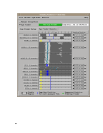
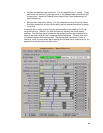
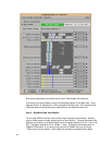
Notice in this display the data valid windows for DATA31-0 and DATA64-32 are reduced
in size. This is because the measured windows represent the intersection of the read
and write windows.
Notice also that there is almost no data valid window for the strobes. This is
unavoidable since the timing of the strobes still shift one quarter clock cycle between
read and write bursts. The data valid window thus shrinks to the natural overlap of the
strobe timings. Signal jitter in real systems usually reduces the window size to zero.
Without the separate analyzer clock timing adjustment for read and write bursts the data
valid window for all data lines would look very much like the strobes.
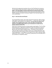
If the eyes for the data lines are less than .5 ns then adjustment of the Read delay line
may be necessary. Also, if this probe is used at different DDR speeds (PC1600,
PC2100, PC2700) adjustment of the Read delay line may be necessary as it is used at
different speeds and/or in different systems. The FS2331 is provided with 2 delay lines,
one of 1200ps (factory configuration) and another of 1700ps, which may be needed for
operation in target systems with slower DIMM bus speeds.
These Delay Lines are very fragile. Be very careful when changing them.
The following procedure should be used to check the delay value. Depending on results,
it may be appropriate to change the Read Delay value to the other value provided. If
neither of these values provides the desired result, please contact FuturePlus Systems
technical Support.
This procedure consists of the following steps:
1. Set the analyzer sample position for DDR commands.
2. Find the data valid window position for write bursts
3. Find the data valid window position for read bursts
4. Adjust the delay line value to maximize overlap between the write and read data
valid windows.
5. Set the analyzer sample positions to the center of the combined read and write data
valid windows.
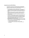
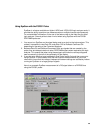
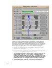
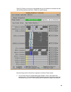
Step 1 – Set Command sample position
For this step the memory bus should be actively carrying DDR commands. Ideally all
the Chip Select lines, address lines, bank select lines, etc. should have activity. Once
the stimulus is running, open the “Setup/Hold…” dialog under the Format tab of the
analyzer receiving DDR commands (for example, slot C). Within the “Setup/Hold…”
dialog select the “Eye Finder” option, and press the “Run Eye Finder” button. Eye
Finder will take about 30 seconds or so to complete, at which time you should see a
display something like the following: