


43
•
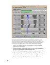
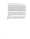
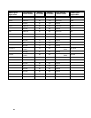
The read strobes straddle the data, as they should for read cycles.
•
The read data valid windows are about the same size as the write ones were. In
many systems however you should not be surprised to find the read windows
appreciably smaller than the write windows. This is due to the physics of the DDR
bus. For read data the analyzer must typically wait for the reflected wave (created
by the DRAM and reflected by the controller chipset) to determine when strobes and
data actually switch. As a result the waveforms are usually much less clean. This
results in an increased amount of jitter in the detected strobe and the data itself.
This shows up as a smaller data valid window for the sampled data. The FS2331
probe incorporates special circuitry and techniques to deal with this as effectively as
possible Because of these signal integrity challenges however the probe may
not be able to reliably capture read bursts under all conditions. The Eye Finder
measurements will tell you which bits may have trouble being sampled most reliably.
•
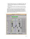
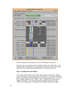
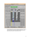
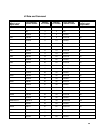
These DIMMs apparently use x8 memories since there is no stable data on the
mask/upper strobe lines. Although there is special circuitry on the probe to deal with
the high impedance state on the DQS0 strobe (which generates the state analysis
clock), the other lines simply sample data using a threshold of 1.25 volts. As a
result when lines are tristated continuously (and so get pulled to the threshold by the
terminators) the analyzer will interpret even small amounts of noise as random 0/1
transitions.
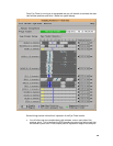
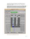
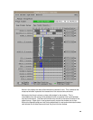
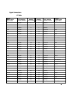
As with write bursts, if Eye Finder chooses the wrong data valid window when selecting
the sample position, move the sample positions to the proper one (just before the
analyzer clock at time 0) before noting the average sample position indicated for the
data lines. After adjusting the sample positions you should see a display like the
following: