


11
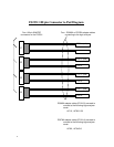
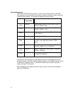
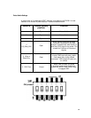
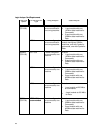
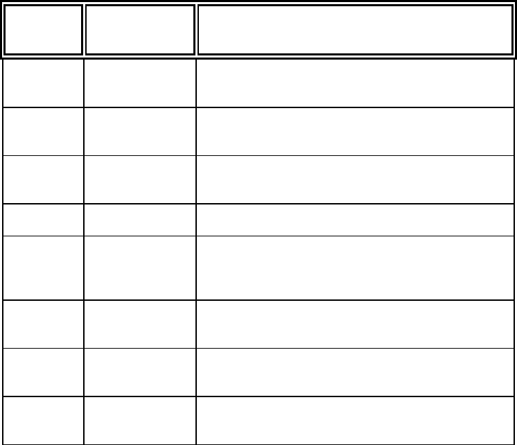
Probe Pod Assignment
The FS2331 DDR Probe uses 8 pods. Two are used to capture traffic on the DDR
Command bus, and 6 are used for the Data bus, strobes, check bits, masks, and Serial
Presence Detect signals. The signals are mapped to pods as follows:
Pod Clock Domain
(Clock Rate)
SIGNAL GROUP
1 Odd
Data (2x) State Analysis Clock (on JCLK), DQ0-3, DQ8-11,
DQ16-19, DQS0-2, SA0
2 Even
Data (2x) Read/Write status (on KCLK), DQ4-7, DQ12-15,
DQ20-23, DQS9-11, SA1
3 Odd
Data (2x) Burst Valid status (on JCLK), CB0-5, DQ24-31,
DQS3, DQS12
4 Even Command (1x) CK0 (on KCLK), A0-15
5 Odd
Command (1x) Buffered Command Clock (on JCLK), BA0-2, S0-
3, CKE0-1, WE, RAS, CAS, Reset, FETEN.
Spare
6 Even
Data (2x) Buffered Command Clock (on KCLK), CB6-7,
SA2, WP, DQS4, 8, 13, 17. DQ32-39.
7 Odd
Data (2x) (Spare – J10on JCLK), SDA, DQS5-7, DQ40-43,
DQ48-51, DQ56-59
8 Even
Data (2x) (Spare – J11on JCLK), SCL, DQS14-16, DQ44-
47, DQ52-55, DQ60-63.
The overlap in the bit ranges for signals between pods occurs because the bits are
assigned to pods in the order that they appear physically on the DIMM connector, which
is not strictly in logical bit order. This allows the probe layout to better match stub
lengths among all DQxx signals.
See the Appendix for a detailed list of how Logic Analyzer Channels are mapped to
signals and DIMM pins.