


MVME55006E Single-Board Computer Installation and Use (6806800A37D)
RAM55006E Memory Expansion Module SROM
48
The RAM5500 SPD uses the SPD JEDEC standard definition and is accessed at address $A2.
Refer to the following section on SROM for more details.
3.3.2 SROM
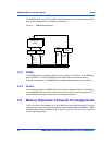
The RAM5500 memory expansion module contains a single +3.3V, 256 x 8, serial EEPROM
device (AT24C02). The serial EEPROM provides SPD storage of the module memory
subsystem configuration. The RAM5500 SPD is software addressable by a unique address.
3.3.3 Clocks
The host board provides one SDRAM clock to the memory expansion connector. The frequency
of the RAM5500 CLKS is the same as the host board. This clock is used to generate the on-
board SDRAM clocks using a phase lock loop zero delay clock driver.
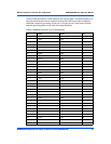
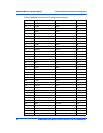
3.4 Memory Expansion Connector Pin Assignments
The P1 connector on the RAM5500 is a 140-pin AMP 4mm Free Height mating plug. This plug
includes common ground contacts that mate with standard AMP receptacle assemblies or AMP
GIGA assemblies with ground plates. Refer to Memory Expansion Connector (P4) on page 86
for the P4 pin assignments.
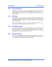
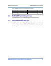
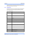
Figure 3-1 RAM500 Block Diagram
A,
BA,
WE_L,
RAS_L,
CAS_L,
DQM
SCL
SDA
A1_SPD
CLK1
CLK (0:8)
A0_SPD
CS_C_L,
CS_D_L
Bank of 9 (x8)
SDRAM
Registers
AVC16722
Registers
AVC16374
SROM
SPD
PLL
Clock
Driver
MVME5500 Mezzanine Connector