MVME55006E Single-Board Computer Installation and Use (6806800A37D)
Connector Pin Assignments VMEbus Connectors (P1 & P2) (SBC Mode)
84
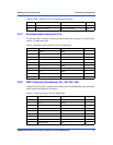
Row B of the P2 connector provides power to the MVME5500 and to the upper eight VMEbus
address lines, and additional 16 VMEbus data lines. Please read the configuration notes below
as they apply to the P2 connector.
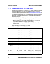
1. When J28 is configured for IPMC mode, –12V is supplied to P2 pin A30. If there is an
incompatible board plugged into this P2 slot, damage may occur.
2. When J32 is configured for IPMC mode, +12V is supplied to P2 pin C7. If there is an
incompatible board plugged into this P2 slot, damage may occur.
3. J102 – J110 should be configured for IPMC I/O to connect the IPMC extended SCSI signals
from J3 to the P2 connector.
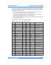
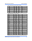
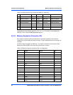
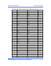
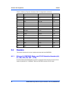
The pin assignments for the P2 connector are as follows:
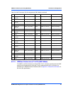
Table 5-17 VME Connector (P2) Pinout with IPMC712
Pin Row Z Row A Row B Row C Row D
1 PMC2_2 DB0# +5V RD- (10/100) PMC2_1 (J24-1)
2 GND DB1# GND RD+ (10/100) PMC2_3 (J24-3)
3 PMC2_5 DB2# N/C TD- (10/100) PMC2_4 (J24-4)
4 GND DB3# VA24 TD+ (10/100) PMC2_6 (J24-6)
5 PMC2_8 DB4# VA25 Not Used PMC2_7 (J24-7)
6 GND DB5# VA26 Not Used PMC2_9 (J24-9)
7 PMC2_11 DB6# VA27 +12V (LAN) PMC2_10 (J24-10)
8 GND DB7# VA28 PRSTB# PMC2_12 (J24-12)
9 PMC2-14 DBP# VA29 P DB0 PMC2_13 (J24-13)
10 GND ATN# VA30 P DB1 PMC2_15 (J24-15)
11 PMC2_17 BSY# VA31 P DB2 PMC2_16 (J24-16)
12 GND ACK# GND P DB3 PMC2_18 (J24-18)
13 PMC2_20 RST# +5V P DB4 PMC2_19 (J24-19)
14 GND MSG# VD16 P DB5 PMC2_21 (J24-21)
15 PMC2_23 SEL# VD17 P DB6 PMC2_22 (J24-22)
16 GND D/C# VD18 P DB7 PMC2_24 (J24-24)
17 PMC2_26 REQ# VD19 P ACK# PMC2_25 (J24-25)
18 GND I/O# VD20 P BSY PMC2_27 (J24-27)
19 PMC2_29 (J24-29) TXD3 VD21 P PE PMC2_28 (J24-28)
20 GND RXD3 VD22 P SEL PMC2_30 (J24-30)
21 PMC2_32 (J24-32) RTS3 VD23 P IME PMC2_31 (J24-31)
22 GND CTS3 GND P FAULT# PMC2_33 (J24-33)
23 PMC2_35 (J24-35) DTR3 VD24 TXD1_232 PMC2_34 (J24-34)
24 GND DCD3 VD25 RXD1 PMC2_36 (J24-36)
25 PMC2_38 (J24-38) TXD4 VD26 RTS1 PMC2_37 (J24-37)


