


iv
ILLUSTRATIONS AND TABLES
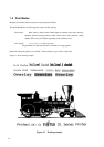
Figure 1.1 Printing samples .............................................................................................................................1-2
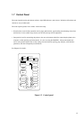
Figure 1.2 Control panel ..................................................................................................................................1-5
Figure 1.3 Cut-sheet feeders ............................................................................................................................1-6
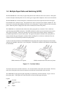
Figure 1.4 Multiple paper paths.......................................................................................................................1-7
Figure 2.1 Printer block diagram .....................................................................................................................2-2
Figure 2.2 Printer components (DL9400 printer) ............................................................................................2-5
Figure 3.1 Printing area for continuous forms.................................................................................................3-13
Figure 3.2 Printing area for cut sheets .............................................................................................................3-14
Figure 4.1 Control panel ..................................................................................................................................4-1
Figure 4.2 Main menu of the DLMENU .........................................................................................................4-3
Figure 5.1 Interface connectors .......................................................................................................................5-1
Figure 5.2 Parallel interface output circuit ......................................................................................................5-2
Figure 5.3 Parallel interface input circuits ......................................................................................................5-2
Figure 5.4 Parallel interface connector............................................................................................................5-3
Figure 5.5 Data transmission timing ...............................................................................................................5-6
Figure 5.6 Serial interface input circuit ...........................................................................................................5-8
Figure 5.7 Serial interface output circuit .........................................................................................................5-8
Figure 5.8 Serial interface connector...............................................................................................................5-9
Figure 5.9 Serial data format ...........................................................................................................................5-10
Table 3.1 Forms size and thickness .................................................................................................................3-10
Table 3.2 Paper thickness by part ....................................................................................................................3-11
Table 4.1 Setup functions ................................................................................................................................4-3
Table 5.1 Parallel interface signals..................................................................................................................5-3
Table 5.2 Serial interface signals.....................................................................................................................5-9