


C141-E090-01EN 5 - 7
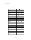
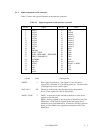
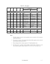
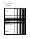
Table 5.3 I/O registers
I/O registers
Read operation Write operation
Command block registers
1 0 0 0 0 Data Data X'1F0'
1 0 0 0 1 Error Register Features X'1F1'
1 0 0 1 0 Sector Count Sector Count X'1F2'
1 0 0 1 1 Sector Number Sector Number X'1F3'
1 0 1 0 0 Cylinder Low Cylinder Low X'1F4'
1 0 1 0 1 Cylinder High Cylinder High X'1F5'
1 0 1 1 0 Device/Head Device/Head X'1F6'
1 0 1 1 1 Status Command X'1F7'
1 1 X X X (Invalid) (Invalid) —
Control block registers
0 1 1 1 0 Alternate Status Device Control X'3F6'
0 1 1 1 1 — — X'3F7'
Notes:
1. The Data register for read or write operation can be accessed by 16 bit data bus
(DATA0 to DATA15).
2. The registers for read or write operation other than the Data registers can be accessed
by 8 bit data bus (DATA0 to DATA7).
3. When reading the Drive Address register, bit 7 is high-impedance state.
4. The LBA mode is specified, the Device/Head, Cylinder High, Cylinder Low, and
Sector Number registers indicate LBA bits 27 to 24, 23 to 16, 15 to 8, and 7 to 0.
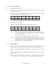
Host I/O
address
DA0DA1DA2CS1–CS0–