


Chapter 1
Introduction
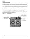
Detailed hp rp7405/rp7410 Description
8
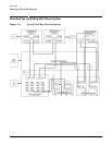
The hp rp7405/rp7410 has a 48V distributed power system and receives the 48V power from the system
backplane board. The cell board contains DC-to-DC converters to generate the required voltage rails. The
DC-to-DC converters on the cell board do not provide N+1 redundancy.
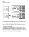
The cell board contains several major buses including:
• Runway buses for each of the four processors
• Two memory buses (one going to each half of the main memory array)
• Incoming and outgoing I/O bus that goes off board to a SBA chip
• Incoming and outgoing crossbar bus that goes off board to the other cell boards
• PDH bus that goes to the PDH/SINC circuitry
All of these buses come together at the CC chip.
Due to space limitations on the cell board the PDH/SINC circuitry resides on a riser board that plugs at a
right angle into the cell board. The cell board also includes clock circuits, test circuits and de-coupling
capacitors.
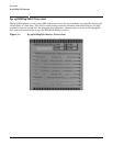
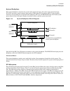
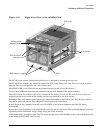
Figure 1-6 shows a simplified view of the memory subsystem. It consists of two independent access paths,
each path having its own address bus, control bus, data bus, and DIMMs. In practice, the CC runs the two
paths 180 degrees out of phase with respect to each other to facilitate pipelining in the CC. Address and
control signals are fanned out through register ports to the SDRAMs on the DIMMs.
Data transferred between the CC and SDRAM passes through custom VLSI circuits (M2) that are bit-sliced;
four form one 72-bit CC memory data bus. These circuits perform speed and width conversion between the
SDRAM and MID busses. They also perform the write (tag update) portion of a read-modify-write (RMW)
access. The CC memory data busses are bi-directional and run at 250 MT/s (million transfers per second).
These links are self-clocked in that a pair of clock strobes is passed along with the data so that phase
realignment can be done by the receiver.
Figure 1-6 Memory Subsystem